
Contact
Write to Us And We Would Be Happy to Advise You.
Do you have any questions, or would you like to speak directly with a representative?
By hqt
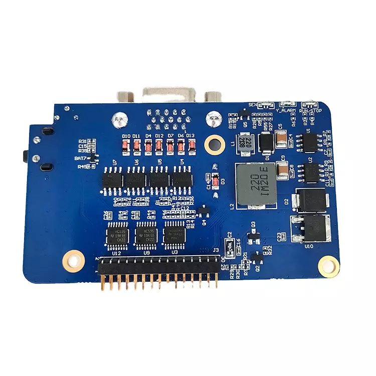
A 4 layer PCB board is a type of Printed Circuit Board that has four layers of conductive material. These four layers are typically made of copper, and are separated by thin layers of insulating material. 4 layer PCB boards are used in a variety of electronic devices, and are especially well-suited for use in high-speed applications.
A printed circuit board (PCB) is a board made of one or more layers of a conductive material, typically copper, that has been etched to form conductive traces, pads, and other features. A PCB allows signals and power to be routed between physical devices. A PCB can be single-sided, with components mounted on one side of the board, or double-sided, with components mounted on both sides of the board.
PCBs are found in a variety of electronic devices, from small handheld devices to large servers. The four main layers of a PCB are:
A Printed Circuit Board, or PCB, is a thin board made of copper clad laminate that is used to mount electronic components. There are four main types of PCBs: single layer, double layer, multilayer, and flexible.
Single layer PCBs are the most basic type of PCB. They are made of a single layer of conductive material, typically copper, with a non-conductive substrate. The conductive material is etched to form the desired circuit pattern. Single layer PCBs are used for simple circuits, such as those found in calculators or digital watches.
Double layer PCBs are made of two layers of conductive material, separated by a layer of non-conductive material. The top layer is typically copper, while the bottom layer can be made of copper, aluminum, or other conductive materials. Double layer PCBs are used for more complex circuits, such as those found in computers or cell phones.
Multilayer PCBs are made of three or more layers of conductive material, separated by layers of non-conductive material. The conductive layers are typically made of copper, while the non-conductive layers can be made of different materials, such as FR4 or polyimide. Multilayer PCBs are used for very complex circuits, such as those found in servers or high-end gaming computers.
Flexible PCBs are made of a flexible material, such as polyimide, with a conductive layer, typically copper. Flexible PCBs are used in applications where the PCB needs to be bent or flexed, such as in wearable electronics.
A 4-layer PCB is a printed circuit board that has four conductive layers separated by insulating layers. The four layers are typically arranged in the following order:
The signal layer is typically the outermost layer, and it is where the traces that carry the signal are routed. The power layer is the second layer from the top, and it is used to distribute power to the different components on the board. The ground layer is the third layer from the top, and it is used to provide a common ground for all the components on the board. The fourth and final layer is another signal layer, and it is used to route signals between the different components on the board.
The fabrication process of a four-layer PCB board starts with the preparation of the Inner layers. The inner layers are the layers that are sandwiched between the top and bottom layers. The next step is to drill the vias. Vias are the small holes that connect the different layers of the PCB. After the vias are drilled, the next step is to etch the copper traces. The copper traces are the lines that connect the different components on the PCB. The next step is to apply the solder mask. The solder mask is a thin layer of plastic that protects the copper traces from being shorted by the soldering process. The next step is to apply the silkscreen. The silkscreen is a thin layer of plastic that is used to print the component names and values on the PCB. The final step is to apply the soldermask. The soldermask is a thin layer of plastic that protects the copper traces from being shorted by the soldering process.
An PCB assembly is a sub section of a main topic, in this case, a 4 layer PCB board. It is made up of many individual parts that must be placed in the correct order and connected together to create the desired circuit. The process of assembling a PCB board can be done by hand, but it is more commonly done using a machine called a pick and place machine.
The first step in the assembly process is to place the individual parts onto the board. This is done by placing the part in the correct location and then soldering it in place. The next step is to connect the parts together using wires or traces. This is done by running a wire from one part to the other and soldering it in place.
After all of the parts are in place and connected, the final step is to test the circuit to make sure it is functioning properly. This is done by sending a signal through the circuit and measuring the response. If everything is working correctly, the Multilayer PCB is now ready to be used in a project.
As the name suggests, a 4 layer PCB has four layers of conductive material that are separated by insulating layers. The four layers are typically arranged in the following order:
The dielectric material can be either a solid sheet of insulation or a thin layer of insulation that is sandwiched between the copper foils. The different layers are connected together using vias, which are small holes that are filled with a conductive material.
The four layers of a 4 layer PCB are typically used for the following purposes:
When it comes to 4 layer PCB boards, packaging is an important consideration. There are a few different ways to package these boards, and the right method will depend on the specific application. One common method is to use a small piece of foam or other material to protect the exposed circuitry. This can be placed under the board or on top of it, depending on the needs of the application. Another common method is to use a clear plastic cover. This can be placed over the top of the board to protect it from dirt and debris. Finally, some companies prefer to use a metal or plastic enclosure. This type of packaging can provide extra protection from the elements and can also help to keep the board from being damaged during shipping.
EMC and Safety are the two main concerns when it comes to the design of 4-layer PCBs. The four-layer stack-up provides excellent isolation between layers, which is essential for EMC control. The inner layers can be used for power or ground planes, which reduces the amount of copper required and thus the cost of the PCB.
However, the four-layer stack-up can also lead to crosstalk between traces on different layers. This is because the four-layer stack-up provides less isolation between traces than a six-layer stack-up. As a result, it is important to carefully route signals on a four-layer PCB to minimize crosstalk.
In addition, the four-layer stack-up can make it difficult to achieve a good ground plane. This is because the inner layers are typically used for power or ground planes, which can lead to ground bounce. As a result, it is important to carefully consider the ground plane on a four-Single-sided PCB
Overall, the four-layer stack-up provides excellent isolation between layers, which is essential for EMC control. However, the four-layer stack-up can also lead to crosstalk between traces on different layers. As a result, it is important to carefully route signals on a four-layer PCB to minimize crosstalk.
A certificate may refer to the physical piece of paper that is issued as proof of certification or it may refer to the process of certification. When referring to the physical certificate, it is a document that states that an individual has completed a course or program and is now certified in a particular area. The certificate may also include the date of certification, the issuing institution and the individual's name. When referring to the process of certification, it is the act of verifying that an individual has the skills and knowledge necessary to perform a certain task or job. Certification can be done through an assessment by a certified body or it can be earned by completing a certification program.
As with any business decision, cost and time considerations must be taken into account when deciding whether to use a 4 layer PCB board. The initial investment for the board and the time required to etch and drill the additional layers may be higher than for a 2 layer board, but the cost savings in terms of routing and shorter design cycles can be significant. In addition, the increased density and complexity that can be achieved with 4 layer boards can offer significant advantages over 2 layer boards, particularly in terms of performance and reliability.
Do you have any questions, or would you like to speak directly with a representative?