
What is a Multilayer Printed Circuit Board?
As it is clear from its name, multilayer PCB is made up of numerous layers of electronic components that are stacked on top of one another on a circuit board with three or more conductive copper foil layers. This printed circuit board has conductive layers of conductive metal with specific copper thickness as it is named multilayer PCB used in complex devices due to its large operating capacity.
These multiple layers of double-sided circuit boards are then glued or joined together with a heat-resistant compound for protection between their layers. Multilayer printed circuit boards come as rigid PCBs. Because it is a very difficult task to design a flexible PCB, the main reason for this is its multiple layers. It is a difficult task to bend numerous layers at any angle simultaneously together.
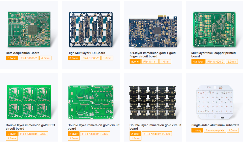
Layer Counts of Multilayer PCB:
Here we can fabricate, assemble and design multilayer boards in different types, like rigid, flexible, rigid-flexible, and metal core PCBs. Each type of multi-layer PCB has a different number of layers in them, depending upon the design requirements.
Rigid Multilayer PCBs: 4, 6, 8, so on up to 30 layers.
Flex Multilayer PCBs: 3, 4, 5, so on up to 8 layers.
Rigid-Flex Multilayer PCB: 2, 3, 4, so on up to 20 layers.
Metal Core Multilayer Boards: 4 layers at most.
Methods of multilayer PCB manufacturing:
Two methods are used for the construction or manufacturing of multilayer circuit boards these days. The through-Hole manufacturing process of placing the electronic components through the holes of the single-layer PCB and then soldering them together was referred to as through-hole construction for the first time to now.
Point-to-Point construction:
When through-hole technology was unsatisfactory for more complex cases during the designing of the PCB, Point-to-Point construction technology was introduced. This proved to be superior to through-hole construction, but it is still not suitable for multilayer PCBs.
Multilayer PCBs construction
The development and construction of multilayer PCBs bring many changes in the world of electronic companies. The development of multilayer PCBs has allowed electronic companies to significantly reduce the cost and also decrease the physical size of their electronic products. The internal connections between the numerous components that make up a multilayer Printed Board Circuit are critical to the device’s functionality. The device is non-functional until and until these components work in tandem. In most cases, the need to improve product performance results in bulky products, but the flexible multilayer PCB design has completely replaced the stiff single-layered PCB design.
Many products, particularly automated and complicated electronics like computers and cellular phones, have enhanced performance thanks to high-quality wiring and flexible parts. However, nowadays technology has progressed to the point where multilayer PCBs can have as many as twenty-four layers, depending on the application and complexity of the device. The majority of our multilayer PCBs include 4 to 8 layers. Smartphones can have as many as 12 levels, depending on the application’s sophistication.
Multilayered PCBs have also made production easier because the majority of them are pre-mounted and prefabricated. Although producing these prefabricated multilayered PCBs is an elaborate procedure, the final stage is now more of an assembly than a manufacturing multilayer PCBs process.
Multilayer PCB development
Although some may believe that multilayer PCBs were extraordinarily efficient because regular PCBs were working perfectly, there are several reasons for their introduction into the market. A multilayer PCB has a more flexible construction and can significantly decrease the size of the electronic device. This isn’t the sole explanation behind this. The cost of producing conventional PCBs was quite high, and costs only continued to rise when new advancements were made. A multilayer PCB, on the other hand, offered simply reprogramming in addition to supplying new innovative onboard components and conductive material. Furthermore, because of prefabricated multilayered structures, mass production has become easier.
Electronic industries have undoubtedly seen an increase in their production rates as a result of the instant installation or assembly of multilayer PCBs. If you are highly concerned about the quality of the circuit board, rest assured that they are well protected and can be used after extended storage. Each board is strictly checked after it is finished to ensure that it performs properly. In case of any kind of failure of the printed circuit board, the procedure of repair is simple and can be accomplished by simply changing the board. It is difficult to restore all the components of the circuit board.
Process and Optimization of Multilayer PCB Manufacturing
The step by step manufacturing of the multilayer PCB is given as follows:
Designing:
It is the first and foremost important step in the construction of multilayer PCB, you need to have an effective printed circuit board design. This design also fulfills all the requirements of the client or customer.
Photo Plotting:
You can plot a film for each layer using a laser photo-plotter. Which helps you to understand the structure of each layer.
Etching:
Apply pads and traces onto the circuit boards.
Automated Optical Inspection:
In Automated optical inspection, you can inspect the designed and actual image on the panel. It helps you to catch any defect in the circuit.
Oxide:
It is a chemical treatment to the inner layer before starting the lamination process.
Lamination:
It is a process to combine different layers of epoxy-infused fiberglass.
Drilling:
This process needs to create a hole to place different components on the circuit boards.
Electronic copper foil deposition:
Deposit a thin layer of copper foil to the surface of the panels.
Dry film outer layer:
This step helps in producing the panel for the electroplate.
Plate:
You need copper foil plating onto the conductive pattern.
Striping and Etching:
In this step, the panel goes through the stripping and etching process.
Solder Mask and Legend:
Apply a solder mask to protect the copper surface.
Surface Finish:
Extra copper is removed from the final product in this step.
Benefits and advantages of the Multilayer PCB:
Multilayer PCBs offer various design advantages from a technological standpoint.
Smaller PCB Size
Multilayer PCBs are naturally smaller than other PCBs. They also have comparable performance and high speed due to the presence of multiple layers.
Lighter PCB Weight
Small size creates a PCB with less weight. This is very useful for today’s devices, which are increasingly focused on portability.
Higher PCB Quality
Multilayer PCBs are of a higher quality than single PCBs due to the amount of complex design and preparation that goes into their fabrication.
More Efficient and Resilient PCB
Due to the high heat bonding and layering process used in their manufacture of multilayer PCBs have many layers of insulation between circuits adding to their strength, efficiency, and resilience.
Single Connection Point:
Multilayer PCBs are designed to work as a singular unit, rather than in tandem with other PCB components. As a result, they have a single connection point, rather than the multiple connection points required to use multiple single-layer PCBs. This proves to be a benefit in electronic product design as well since they only need to include a single connection point in the final product. This is particularly beneficial for small electronics and gadgets designed to minimize size and weight.
Applications of Multilayer
PCB:
Multilayer printed circuit boards are highly superfluous, they are used in multiple technologies and have a very wide area of application. Such as:
- Mobile phones – Smart Phones,
- Satellite Communications,
- GPS Satellite Systems,
- Cell Phone Signal Transmission,
- Medical Electronic Devices,
- Weather Technolgy,
- Automotive Industry
- Monitoring, and Data Cloud Storage.
- Atomic accelerators
- File servers and data storage
- Heart monitors
- Fiber optic receptors.
- Cat scan technology and other X-ray equipment
- Repeaters and cellphone transmission
Choosing the Right Manufacturer for Multilayer PCB:
Manufacturing a multilayer printed circuit board requires specialized equipment and a significant commitment to operator training, not to mention the financial consideration when the board with complex design. This explains why some PCB fabricators have been slower to step into the multilayer boards production market than us. MOKO Technology can provide the advanced capabilities to support advanced PCB designs with demanding requirements including laser-ablated micro via, embedded passive boards, heavy copper PCB, via in pad, high-frequency boards, and others.
Things You Should Know Before Choosing Multilayer PCB Manufacturer:
You must be familiar with the different pros and cons of multilayer circuit boards. Moreover, you must know that multilayer board are compatible with your application. If multilayer printed circuit boards are applicable for your product, you need to choose the best manufacturer. You should look for the following thing while hiring any company for multilayer PCB manufacturing:
· Always look for product quality.
· Compare the prices of different companies before placing the order for multilayer PCB manufacturing.
· Look at the minimum quality. Most companies don’t give compensation for the low volume.
· You should also consider customization options.
· Customer support is another important factor to consider.
Multilayer PCB Fabrication with EuropePCB
It is very difficult to design and manufacture multilayer circuitry. If manufacturers are proficient, it is not a big deal. So, are you looking for Multilayer PCB China? EuropePCB is the best option to consider for multilayer PCB boards. You will get the highest quality to produce multilayer PCBs at fair prices. For high-volume PCB, you will have a good concession. This is even an ideal platform for low-volume PCB manufacturing. We'll be with you every step of the way throughout the process of producing your multilayer PCB, providing expertise and advice when needed. Our experienced team has produced thousands of multilayer PCBs varying in design and complexity.