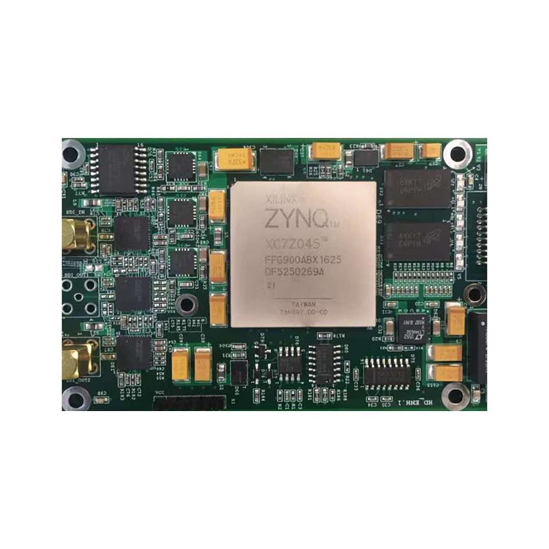
The growth in the industrial sector is exponentially increasing to such an extent that we find too many suppliers and manufacturers in a particular sector say the automobile sector. Similarly talking about electronic PCB manufacturing services, there are a large number of CEM (Contract Electronic Manufacturers) that provide services in this domain and Automated Optical inspection AOI. Some of them are simply the bare PCB manufacturers only, some of them are PCB Assemblers, some are turnkey solution providers i.e. they provide PCB mass manufacturing plus PCB assembly and also provide value-added services in later stages after the PCB is fabricated and stuffed and finalized.
Inspection of PCB
A very important in-process step while fabrication of PCBs is the inspection of PCB. This is inevitable in today's complicated circuit design-based PCBs where hundreds of components are stuffed upon the PCB to implement the inspection procedure. However, there are commonly three types of inspection methods. Visual inspection, AOI, and AXI (Automated X-ray Inspection).
When it comes to inspection methods for PCBs and PCBAs, the manual inspection did make sense for some time. Nevertheless, it is hardly acceptable for inspection of modern circuit boards since it fails to inspect their internal issues or defects.
What is Automated Optical inspection AOI? and Why is it needed in PCBs and PCB assembly?
AOI, as the name suggests, is an automated method of inspecting printed circuit boards during manufacturing. AOI setups typically include multiple high-definition, high-definition, and zoom cameras with powerful light sources, main processing, memory, and operators.
PCBs today typically start in four layers, so components are packed densely on the board, so AOI must be done at different stages of the PCB manufacturing process. AOI can be performed on both bare PCBs and PCBs with components assembled. AOI is important to detect errors, defects, and anomalies at an early stage to ensure the quality of the PCB according to the standard, stop the process, correct the errors, and then resume the process. This helps to reduce PCBs with too many defects at the end of the process. This reduces the number of counterfeit PCBs and lowers the overall manufacturing cost. Typically, AOI is performed after reflow soldering to detect defects in solder joints early in the production line.
Attributes and Capabilities of Automated Optical inspection AOI Test
Depending on the visual method, AOI testing can be applied to detect a variety of surface defects including scratches, nodules, stains, breaks, short circuits, insufficient or excessive solder, faulty components, missing components, the incorrect polarity of components, and more. AOI Allows passing through passive visual control elements that were used primarily before the popularization of AOI but can be performed quickly and accurately.
Multi-object:
AOI testing is suitable for both bare PCBs and PCBs. Check the PCB for defects such as short circuits, open wires, lack of solder, etc. Check for issues including component soldering, polarity, and values for PCB validation.
Flexibility:
Automated optical inspection can be configured at any stage of the production line according to customer needs and costs. Most defects are caused by inconsistencies that occur during the soldering process, so placement after reflow soldering is best to increase inspection efficiency and reduce associated costs. The flexibility property of AOI testing is cost-effective because it is being tested, and if problems are found, production or assembly parameters can be changed immediately to ensure that subsequent products are produced correctly. As a result, products are no longer rejected during functional testing or final inspection.
Low Cost:
Compared to automated X-ray inspection, post-flow AOI is less expensive to inspect defective solder joints, including straps, broken joints, dry joints, etc.
Precision and Reliability:
The most reliable and accurate system of results.
AOI Operation:
The AOI inspection is performed by scanning the PCB surface. The AOI machine is equipped with an HD color camera that scans the surface at high magnification, clearly showing details about each section of the PCB and each component in each section on a large monitor screen. The camera captures an image of the PCB surface through a light source such as a fluorescent or LED lamp, UV or infrared. The images are then compared to pre-programmed data and loaded into the memory of the AOI processing system.
If a tolerance limit is found to be exceeded, the difference or normalized cross-correlation (NCC) is displayed and displayed, and the process stops immediately. The higher the NCC, the smaller the difference between the captured image and the pre-programmed (template) image. The final decision to declare a board defective and stop the process depends on various algorithms running on the AOI machine, depending on the number of pixels and the NCC value.
Function of Automated Optical inspection AOI
The operator of the AOI machine also visually checks the image captured by the AOI machine on the screen, allowing the process to be stopped manually if deemed necessary. Droplet analysis is done by isolating an image of an object from its background and then incorporating or grouping "droplets or pixels" of the image based on pixels and troubleshooting. AOI can be performed before reflow to check the placement, location, and condition of the part, i.e. non-solder defects. After reflow, the AOI detects defects in the solder joints, components, and the PCB itself that can occur due to the thermodynamics of the
reflow oven.
The AOI machine not only handles ICs but also the smallest components such as 01005, 0201, and 0402 housings. You can scan. housing. For surface inspection only, not package inspection such as QFP, QFN, CSP, BGA, and PoP. The components below the IC case/package cannot be found in AOI. AXI is required for this. X-rays can penetrate the body, so they can display a grayscale image to identify components under the IC housing.
The types of defects AOI can identify:
The AOI is an impressive way to automatically inspect printed circuit boards on a high-volume production line. AOI is open and short, the incorrect polarity of components, incorrectly installed or missing components, incorrect IC package orientation, smudges, cuts, scratches, insufficient solder paste, solder straps, cracked solder joints, excess solder, raised You can check the leads. , Zeolite, Solder Ball, Billboard, Packaging Height (3D AOI), Coplanarity (3D AOI),
Why AOI preferred over Visual Inspection method:
There are many reasons to choose AOI over visual inspection. However, visual inspection is still performed by many PCB companies. The main reasons for choosing AOI before visual inspection are:
1 The human eye can be fatigued, and fatigue is common when visually inspecting small components on a PCB. A car, on the other hand, is neither tired nor tired.
2 Visual inspection is error-prone and can inadvertently miss defects on the PCB. An AOI machine, on the other hand, will not miss a defect if these defect details are programmed into the AOI machine's memory. Therefore, AOI accuracy is better than visual inspection.
3 People can get tired of doing the same thing, but a machine can do the same thing over and over forever.
4 AOI is useful for batch production for PCB manufacturing and assembly, but visual inspection is not suitable for mass production, it is suitable for prototype level production.
5 AOI is faster and can save time and money, but visual inspection is slower and requires more focus and inspection completion time.
6 AOI is a machine-based inspection method, therefore It provides a valuable record for Multiple visual inspections that do not record types of malfunctions and defects, but can be easily corrected. The
7 AOI ensures that the PCB is completely free of defects and there is always the possibility that some defects remain on visual inspection.
In summary, AOI is an important aspect of PCB manufacturing and assembly. It can be flexibly implemented at any stage of the process according to user requirements or requirements. For mass production of complex SMT PCBs, AOI is highly recommended.
AOI Test from Europe PCB:
Why Europe PCB is the top choice for Automated Optical inspection AOI?
AOI is a major inspection method for PCB assembly. It quickly and accurately inspects errors or defects that occur during the PCB assembly process to ensure high-quality PCB assembly without defects after shipment from the conveyor. . AOI can be applied to both bare PCBs and PCB assemblies. However, in Europe, PCBs are primarily used to test SMT assembly lines, and nail and flying probes are instead used to test non-nail PCBs.
Model ALD515 uses the EuropePCB professional automatic optical inspection machine.
EuropePCB provides both online and offline AOI testing to meet different customer requirements. Online AOI testing is more automated and does not require manual control, whereas offline AOI testing is less automated and requires manual control. However, both use the same validation principles, validation objects, and validation methods. We are always here to help you, when you contact us, Our expert team with years of experience answers your queries.