Through-hole Technique (also known as “penetration”). Through-hole wiring is a wiring process in which component leads are inserted into drilled holes on an uncoated PCB and soldered to opposite pads. This can be achieved using manual assembly or automatic setting machines. Solder joint quality is important for several reasons. Solder joints are the actual connections between components and boards. The quality of the soldered joint is the same as that of the joint. The shape of a solder joint is less important, but generally indicates the quality of the solder joint.
Background and History of Through-Hole Assembly:
Through-hole technology once dominated electronic assembly methods from the 1950s through the 1980s when surface mount technology (SMT) came to prominence. During that time, every component on a PCB was a through-hole component. Since then, SMT has been widely adopted due to its advantages and changing technical requirements for TH components. However, TH is still a common method used to carry electrical connections from one layer to the next (think breakout boards and header pins).
PCB had to be routed at first on one side and then on both sides, later PCBs with multiple layers were added. A via or Plated through-hole (PTH) is then designed to make contact with the conductive layer.
Characteristics:
Through-hole mounting provides a stronger mechanical connection compared to surface mounting methods, but requires additional drilling and therefore costs more to manufacture the PCB. Because the holes must go through all layers in opposite directions, they also limit the routing area available for signal traces in the layer just below the top layer of the multilayer board. To this end, current push-through methods are generally reserved for bulkier or heavier components such as electrolytic capacitors or semiconductors in larger packages such as TO-220, or components such as plug connectors or electromechanical relays, which require additional wiring strength. there is. . support.
When prototyping, design engineers often prefer larger parts over SMD parts because they can be easily used with breadboard connectors. However, high-speed or high-frequency designs may require SMT techniques to minimize stray inductance and capacitance of lead wires that can degrade circuit performance. The ultra-compact design can define the design of SMT even at the prototype design stage.
Some other features of the through-hole assembly
· High reliability
The high reliability of the Thru-Hole assembly provides a higher environmental footprint as the components are secured to the board by pins inserted through holes instead of simply soldered to the PCB surface with SMT components. Therefore, thru-hole assembly is the preferred process in the military and aerospace industries with high-reliability requirements as it provides a more reliable physical connection.
• Ease of Manual Operation:
This assembly method is widely used in PCB testing and PCB prototyping applications because parts are easier to replace or relocate.
• Increased durability:
Due to its high-temperature resistance and resistance to high loads, it is often used in industrial machinery and equipment through parts. The through-hole LEDs are very bright and durable, so you'll find them in the LED lights on huge billboards.
• Lower Manufacturing efficiency:
The additional step of pinning parts with the drill is time-consuming for downhole assembly, increasing costs and reducing production efficiency.
• Restricted PCB Design:Through-holes are not suitable for multi-layer PCBs. This is because the PCB layout and manufacturing design are complicated as the drilled holes must cover all layers of the PCB. Also, the overall board size is larger than the SMT PCB, which makes the application more limited.
Advantages of through-hole assembly:
Here are some advantages of using through-hole assembly while manufacturing PCB.
Easy Prototyping:
It is the best technique for PCB prototyping and testing because components of through-hole can easily be swapped out.
Protection from high heat:
Through-hole assembly is the best choice for manufacturing aerospace and military products because of its high tolerance to heat.
Excellent power handling capacity:
Soldering components by through-hole technology have a stronger bond with the printed circuit board. So that’s why it is preferred in manufacturing and designing for the larger components such as:
- Mechanical stress
- High voltage
- High power
These are the important attributes of the transformer, heavy-duty connectors, and also for electrolytic plating in multiple processes.
Strong Physical Connections:
In through-hole technology, components are solder on the opposite side of the printed circuit board so they can withstand environmental stress. Because they have a stronger physical connection via through-hole technology.
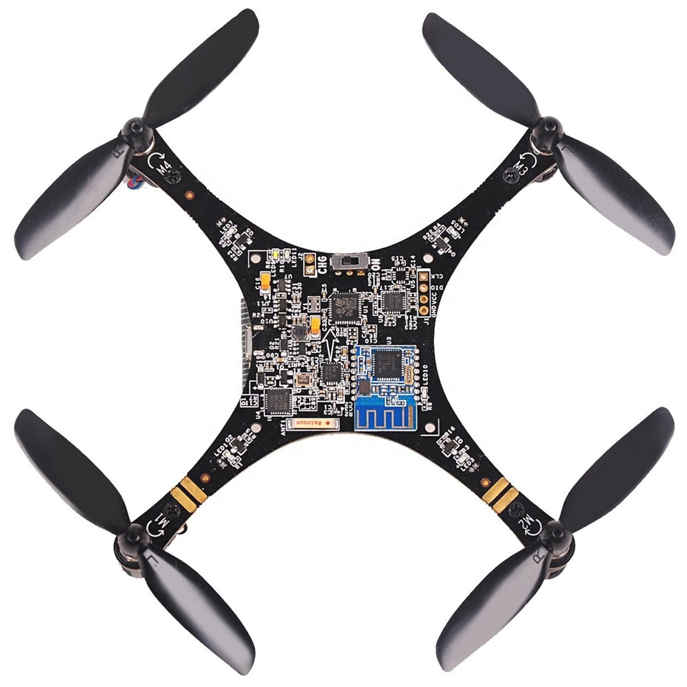
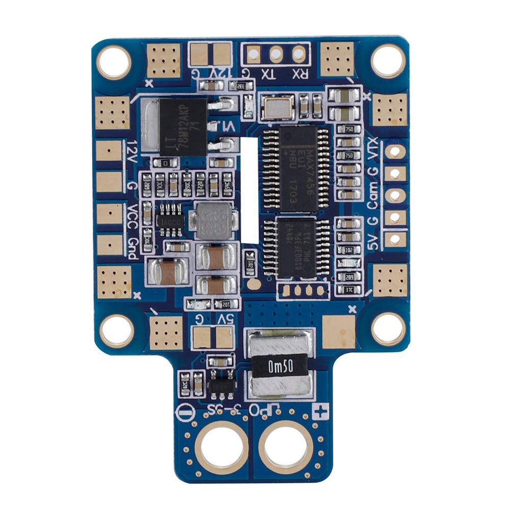
Through-Hole Components:
There are two types of through-hole components: axial and radial. All of these components are "double lead" components with obvious advantages.
• Axial components:
Axial lead components have the end of the lead wire exiting the component straight through the component at both ends (along the "axis"). Then screw both ends through the two separate holes in the board for a tighter and flatter fit. These components are preferred when a tight, compact fit is desired. Axial lead configurations can be in the form of carbon resistors, electrolytic capacitors, fuses, and light diodes (LEDs).
•Radial components:
A component with a radial pin is protruding from the board and the pin is on one side of the component. Radial leads take up less surface area and are preferred for high-density slabs. Radial components are available as disk ceramic capacitors.
Techniques of Through-hole assembly:
We use both automatic and manual methods to place PCB components. Typically, parts for holes are placed manually, while surface set components are placed using grippers and setters. In most cases, a small number of printed circuit boards cannot be assembled automatically.
The soldering methods my team uses are wave soldering through components and reflow soldering to surface mount components. The through-hole assembly process places the components on the PCB and wave soldering is used to solder the component leads into the through-holes. In the SMT assembly process, solder paste is applied to the PCB through a solder stencil, then the components are placed on pads and processed in a reflow oven to melt the solder paste. Also in mixed technology, PCB is wave fusion and fusion.
After soldering, PCB, we use the latest technology to clean the assembled PCB from all flux residues. In addition, a variety of methods are used to remove flux residues, typically a combination of cleaning agents, stirring, and heating. Then the PCB is sent for detailed inspection to confirm the correct placement of the components. State-of-the-art inspection tools are used to check the quality of assembled boards. Methods used to include sample inspection, automated optical inspection (AOI), and X-ray inspection. They go through rigorous quality testing before being shipped to the end-user.
What is the difference between through-hole assembly and SMT assembly?
The through-hole assembly process places the components on the PCB and wave soldering is used to solder the component leads into the through-holes. In the SMT assembly process, solder paste is applied to the PCB through a solder stencil, then the components are placed on pads and processed in a reflow oven to melt the solder paste.
From the introductions listed above, it can be concluded that surface mount assemblies are more efficient and cost-effective than downhole assemblies. Modern electronics have witnessed the use of SMT in most electronics. However, downhole installation is still important given its special mechanical, electrical, and thermal properties.
Science and technology are constantly advancing and old products are replaced with new ones, but this does not mean that old technology should be eliminated. For example, a multi-layer PCB is more advanced and more complex than a single-layer PCB, but would you like to utilize it in a watch or a simple toy? The answer is 'No. The merits of some older schools may still be the main reason they will play a role in the future.
Types of Through-hole assembly components:
Single-ended:
This is mostly used in integrated circuit embedded systems. Those ICs that have terminals in one single file are said to be single-ended THT components.
Double-ended:
Again, it is applied in ICs systems. Some IC for example the 8051 AT89C51 has pins that are arranged in two files each from its side of the length as shown below. The type of THT that will be used to fix them in the PCB is called double-ended THT mounting.
Pin Grid arrays THT:
In this type of THT, the components have so many pins that are arranged throughout the components. In this type, there will be drilling of so many different size holes throughout the spacing that is designated for the components.
Why Europe PCB is the best choice for Through-hole assembly?
Due to the rapid development of technology, some production methods are gradually being phased out. Existing methods, such as downhole techniques, may have limitations, but still have some advantages over newer techniques. Downhole technology has a proven track record of durability and reliability. Europe PCB offer semi-automated, fully automated, and manual setup methods for downhole assembly. Contact us for more information on through-hole technology for your PCB projects.
PCB Technical Specification
|
|
Order quantity
|
1-500,000
|
|
Number of layer
|
1,2,4,6,up to 22 layers
|
|
Board material
|
FR-4, glass epoxy, FR4 High Tg, Rohs compliant, Aluminum, Rogers, etc
|
|
PCB type
|
Hard, flexible, rigid-flexible
|
|
Shape
|
Any shape: Rectangular,round,slots,cutouts,complex,irregular, etc
|
|
Max PCB dimensions
|
20inch*20inch or 500mm*500mm
|
|
Board thickness
|
0.4~4.0mm
|
|
Thickness tolerance
|
± 10%
|
|
Copper thickness
|
1/2OZ 1OZ 2OZ 3OZ
|
|
Copper thickness tolerance
|
± 0.25oz
|
|
Solder mask
|
Green, red, white, yellow, blue, black, etc
|
|
Silk screen
|
White, yellow, black, or negative, etc
|
|
Silk screen min line width
|
0.006'' or 0.15mm
|
|
Surface finish
|
HASL, Nickle, Imm Gold, Imm Tin, Imm Silver, OSP etc
|
|
Min drill hole diameter
|
0.01'',0.25mm.or 10 mil
|
|
PCB cutting
|
Shear,V-score,tab-routed
|
PCB Assembly Capabilities
|
|
SMT Jointing Min. Space
|
0201mm
|
|
QFP Space
|
Pitch 0.3mm
|
|
Min. Package
|
0201
|
|
Min. Size
|
2*2 inch(50*50mm)
|
|
Max. Size
|
14*22 inch(350*550mm)
|
|
Placement Precision
|
±0.01mm
|
|
Placement Precision
|
QFP, SOP, PLCC, BGA
|
|
Placement Capability
|
0805, 0603, 0402, 0201
|
PCB Lead time (workday(s))
|
|
|
|
|
|
|
|
|
Sample Lead time (Normal)
|
|
|
|
|
|
|
Sample Lead time (Faster)
|
|
|
|
|
|
|
Mass production lead time
|
|
|
|
|
|
|
|
|
Sample Lead time
|
PCB Fab+Components Sourcing+PCBA=15 workdays
|
|
Mass production lead time
|
PCB Fab+Components Sourcing+PCBA=20 workdays
|