
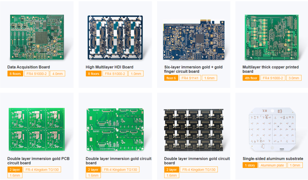
Everything You Need to Know about HDI PCB:
High-density interconnect, or HDI, circuit boards are printed circuit boards with a higher wiring density per unit area than traditional printed circuit boards. In general, HDI PCB is defined as PCBs with one or all of the following: micro via; blind and buried vias; built-up laminations, and high signal performance considerations. Printed circuit board technology has been evolving with changing technology that calls for smaller and faster products. HDI boards are more compact and have smaller vias, pads, copper traces, and spaces. As a result, HDIs have denser wiring resulting in lighter weight, more compact, lower layer count PCBs. Rather than using a few PCBs in a device, one HDI board can house the functionality of the previous boards used.
HDI design
HDI requires the latest advances in the PCB interconnection technology: With the latest state of the art HDI technology, HDI PCBs can be defined as those printed circuit boards that make use of some or all of the following features; Blind and buried via or micro via techniques, high signal performance considerations, micro vias, and built-up standard PCB laminations. Higher connection pad densities or HDI technology came into the limelight close to the end of the 20th century. Its popularity grew tremendously due to the numerous advantages it holds over traditional PCBs. The advanced multilayer deployed by HDI printed circuit manufacturing allows you to integrate multiple layers to create a multi-layered PCB.
What is Micro-Via?
In HDI PCB, micro-vias interconnect HDI substrates and printed circuit board layers to adapt to the high input/output (I/O) density of advanced packaging. HDI utilizes this micro via geometric structure finer lines technology to make circuits that can improve the efficiency of assembly and space utilization and is also necessary for the miniaturization of electronic products in fewer layers.
Difference between conventional PCB and HDI PCB
The following are the three major areas in which you can see variations between ordinary and HDI PCBs:
· The density of the circuit – When the designers build HDI PCBs, they often choose to cover the wires that link to the next layer. You can use micropore processing to do this. It will allow you to maximize the PCB circuit density, which can be useful for small electronic applications.
· Manufacturing technology - HDI PCBs are once again relying on advanced micropore technology, particularly in comparison to the traditional drilling procedures that standard PCBs utilize during manufacturing.
· Electrical performance and signal – HDI PCBs micropore contacts lead to a high level of interruption security, which provides safety from signal interferences. It is one reason you can improve the performance of an HDI board over a raw PCB.
What are the advantages of HDI PCB?
Generally, HDI circuit boards have the following advantages:
Reduce the PCB cost: When the density of printed circuit board increases by more than eight layers, it will be manufactured by HDI high-performance thin materials, and its cost will be lower than the traditional complicated lamination process Increase circuit density: The interconnection of traditional circuit boards and parts must be connected through the lines and via-hole conductors drawn out around the QFP (fan-in and fan-out), so these circuits need to occupy some space.
The micro via technology can hide the wiring required for interconnection to the next layer. The connection between the pads and the leads between different levels is directly connected by the blind holes in the pads, without the need for fan-in and fan-out wiring. Therefore, some pads (such as mini-BGA or CSP small ball bonding) can be placed on the outer layer board to accept more parts, which can increase the density of the circuit board. Many high-function small-sized wireless phone handset boards use this new stacking and wiring method. Conducive to the use of advanced assembly technology:
Generally, the traditional drilling technology cannot meet the needs of small parts of the new generation of thin circuits due to the size of the pad (through-hole) and mechanical drilling. With the advancement of micro via technology, designers can design the latest high-density IC packaging technology, such as Array package, CSP, and DCA (Direct Chip Attach), into the system. Better electrical performance and signal accuracy:
The use of micro-hole interconnects can reduce signal reflection and cross-talk interference between circuits, and allow more space for the circuit board design. Due to the physical structure of the micro-holes, The nature is that the holes are small and short, so the effects of inductance and capacitance can be reduced, and the switching noise during signal transmission can also be reduced. Higher reliability: Due to the thinner thickness and aspect ratio of the micro-holes, the reliability of signal transmission is higher than that of ordinary through-holes.Improved thermal properties:
The insulating dielectric material of HDI boards has a higher glass transition temperature (Tg), so it has better thermal properties. Improve radio frequency interference/ electromagnetic wave interference/electrostatic discharge (RFI/ EMI/ ESD): micro via technology can allow circuit board designers to shorten the distance between the ground layer and the signal layer to reduce radio frequency interference and electromagnetic wave interference; on the other hand, the number of ground wires can be increased to avoid damage to the parts of the circuit due to the instantaneous discharge caused by static electricity accumulation.
Increase design efficiency:
The micro via technology allows the circuit to be arranged on the inner layer so that the circuit designer has more design space, so the efficiency in circuit design can be higher.
HDI PCB Applications
HDI boards are appropriate for a wide range of industries. As mentioned above, you'll find them in all types of digital devices mobile devices, mobile phones, digital cameras, laptop computers, tablets, and more components where miniaturization is key to the effective application of the product. You can also find high-density interconnect PCBs in automobiles, aircraft, and other vehicles that rely on electronics. One of the most critical areas where the high-density PCB is making huge inroads is in the medical arena. Medical devices frequently need small packages with high transmission rates that only HDI PCBs can supply.
For example, an implant needs to be small enough to fit in the human body, but any electronics involved in that implant absolutely must efficiently allow for high-speed signal transmission. Here, the HDI PCB indeed is a godsend. HDI PCBs can also be useful in other medical equipment, like emergency room monitors, CT scans, and much more. No matter your industry, you're probably already getting some ideas about how high-density interconnect PCBs can make the electronics you produce or use even better - get in touch with us PCBCart to discuss it. We'll let you know if you're on the right track and help you decide exactly how beneficial an HDI PCB can be to your industry. Then, you can determine whether or not to take the next step.
HDI Structures
There are mainly two HDI structures:
· Buildup
· Any-layer
Buildup Structure
The buildup structure, which is the basic structure of HDI PCB, uses mechanical drilling as well as laser drilling. Firstly, the core is laminated, drilled by mechanical drilling, plated, and filled. Subsequently, additional micro-via layers are added to the core, and then the drilling, plating, and filling processes are repeated. The buildup structure has a formula of N+C+N. N and C respectively represent the number of micro-via layers on either side of the core and the core. It has a through-hole via to connect outer surfaces and another one inside the core drilled before adding HDI layers. In the 2-layer of high-density interconnection, stacked micro-vias are copper-filled.
Any Layer Interconnection Technology
Any layer interconnection technology is an advanced technology used in HDI design. It is mainly for high-level interconnection applications since any of the two layers in the PCB can be interconnected without any restriction. In other words, any-layer technology has higher flexibility in the layout, which saves the PCB space at least 30%. However, due to its complexity regarding technology, the cost is higher than conventional buildup boards. Unlike the buildup structure, the micro-via is first drilled in the layer by laser drilling, followed by repeating processes of copper-plated, inner-layer image transfer and press, and the outer-layer imaging transferring finally.
Why choose EuropePCBfor HDI Printed circuit boards?
EuropePCB is the leading expert at PCB design, embedded engineering, PCB manufacturing, and PCB assembly in China. We provide PCBs from a 2-50 layer for fabrication, which includes HDI, Flex, Rigid, multilayer PCB, and Rigid-flex boards. We also offer from low quantity to mass production, with high quality available at a low cost. So if you are looking to get the best and affordable HDI PCB manufacturing service, why don’t you order from EroupePCB. We can optimize your designs and calculate tolerances that will allow you to adjust the HDI PCB designs with high reliability. This, too, without influencing its fitness for your particular application.