
Contact
Write to Us And We Would Be Happy to Advise You.
Do you have any questions, or would you like to speak directly with a representative?
By hqt
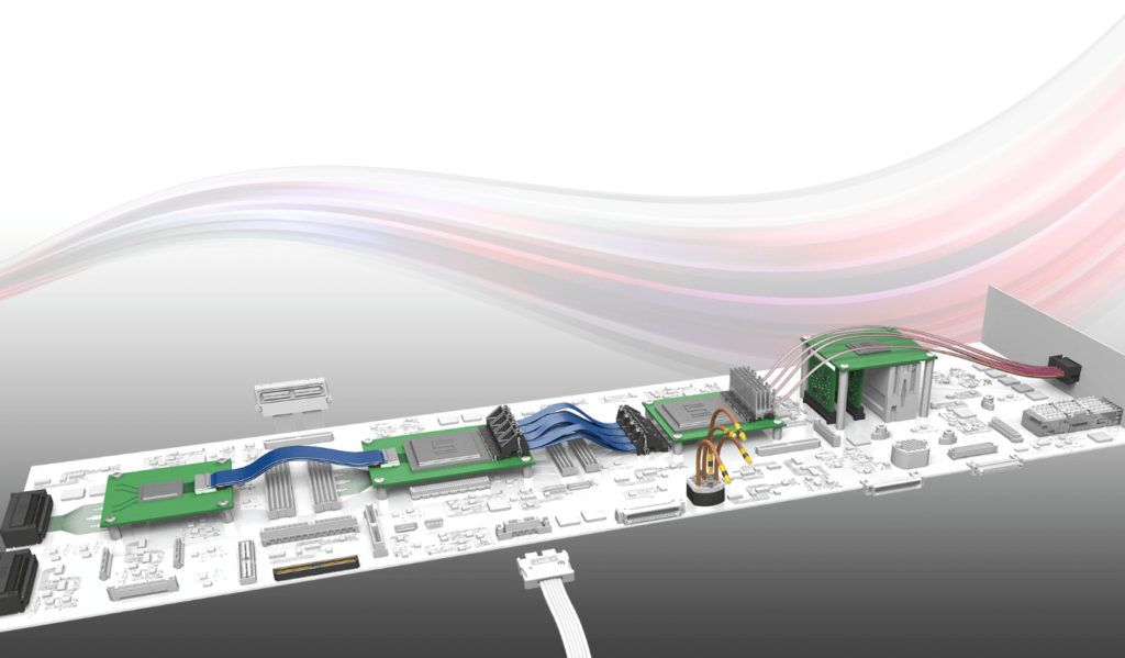
Communication PCB board holds great importance in the telecommunication industry. PCB boards have helped revolutionize the industry. They now are an imperative part of all aspects of the telecom industry, signal boosting online systems being on top.
Modern and sophisticated Printed Circuit Boards have the ability to enhance signal integrity. However, at the same time, if you do not pay heed to their design, they can result in transmission issues. You might face poor signal integrity and a lack of speed.
Something, you would want to avoid at all costs, especially now when the world is shifting to 5G. With every passing day, wireless connectivity is becoming faster, thus it is important to maintain efficiency. After all, the losses related to Printed Circuit Board Transmission lines hold great importance in the area of signal integrity and high-speed design/simulation.
Traditionally, digital designs did not face issues because of transmission line effects. However, now it seems that they have certain issues including lower speeds and lower frequencies.
Due to lower frequencies, the signal integrity stays intact as the signal remains within the data characterization. Thus, allowing the system to perform efficiently. The system is able to fulfill all the desired functionality without any trouble.
Nonetheless, the increase in system speeds results in a greater impact of higher frequency on the system. The effect is not limited only to the digital properties of the system. On the contrary, it starts showing its impact on the analog features within the system.
Therefore, you would have to consider both the digital as well as the analog effects of the system. Among the biggest challenges of signal integrity, you have the challenge surrounding I/O signaling. This is the place where the data that is being sent can be affected by the transmission lines.
These lines can really lower the quality of the data. Therefore, catering it well before time is important to ensure signal quality.
There is little to almost no influence of the frequency response on the signal, in the case of lower speeds. The rule doesn’t hold well if you are sending the signals via a long transmission medium. But, the increase in speed, consequently allows the high-frequency effects to take over.
Despite the length of the transmission medium, higher lower causes problems like crosstalk, ringing, ground bounce, and reflections. All this has an adverse impact on the response of the signal. It tends to signal to hamper in, thus hurting the signal integrity.
Even though these problems are big, you can overcome them effortlessly. Just make sure that you follow good designing techniques for the PCB. The guidelines below will help you design Printed Circuit Boards that would enhance the signal integrity instead of damaging it.
Below, we have come up with effective guidelines after doing thorough research. These guidelines have been published in a number of sources including Texas Instruments. The majorly addresses high-speed signals.
For instance, they would focus on the clock signals along with their routing. The idea is to give a PCB designer a review of the vital coherences. After all, there are several factors that can have an adverse impact on the transmission lines.
For instance, you might end up with EMI problems. Nonetheless, it is possible to not only overcome but also reduce the chances of their occurrence by ensuring the right PCB design. With correct and effective Printed Circuit Board designs, the designer can effortlessly minimize these problems.
What if the fastest rise time and the highest frequency time in the system?
Is it possible to route the sensitive signals, for instance, termination, controlled impedance, and trace propagation delay?
Determine the electrical specifications at the outputs as well as the inputs of the sources and sinks.
You can avoid using the stripline technique by incorporating the microstrip for sensitive signals? Or the stripline technique is imperative.
It is important to create a system’s functional group diagram. For example, digital signals, analog signals, receiver paths, transmitter paths, and many more.
Find out the different supply voltages that exist. In addition, acquire information that whether you would need a power plane for every supply voltage or you have the facility of splitting among them.
Determine whether there an interconnection exists between two independent functional groups. In case, there is a connection, you would have to be extra careful with them. Focus on the return current as well as the crosstalk to some other traces.
Make sure to clear the minimum separation, height, and wider of the trace with your selected Printed Circuit Board manufacturer. Also, determine the minimum distance that you would want or can afford between two layers.
Focusing on the minimum requirements and drills of the vias is another important aspect of a Printed Circuit Board.
Is there a possibility of using either the buried or the blind vias?
A right angle in the trace generally results in more radiation. There is an increase in the capacitance in the region corner, thus a change occurs in the characteristic impedance. The impedance results in ina change in reflection.
So, to avoid these issues, we recommend that you do not incorporate right-angles in the traces. A better option is that you route them a minimum of two 45-degree corners. Furthermore, you minimize the impedance changing by an effective routing technique. That is, you use the round bend.
Pay close attention to placement and ensure separation between low-speed signals and high-speed signals such as clock signals. Similarly, keep the analog signals and the digital signals separate.
It is possible to minimize crosstalk between 2 signals of a layer by routing them to 90-degree from each other. Moreover, the 90-degree routing can also eliminate this issue among two adjacent layers.
You cannot avoid using vias as they are imperative for most routings. However, it is the designer’s job to be careful with them. Vias add extra capacitance and inductance. This, resulting in reflection, which then leads causes a change in the characteristic impedance. Not only this, but vias also result in an increase in the trace length.
When you are using different traces, we recommend you avoid using vias.
When building a Printed Circuit board, the design greatly depends upon the packages that you use for the designing purpose. In addition, you would have to consider the impedance matching requirements and the desired signal trace density.
It is mandatory to use a multilayer Printed Circuit Board with power supply planes and buried ground. The Communication PCB Board is to be a high-speed board. The incorporation of Solid copper planes permits the designer to keep the power connections short and the device ground.
Moreover, with the ground plan, it is possible to achieve low inductance for high-speed signal’s return paths.
When it comes to PCB lamination, the industry has developed immensely. Designers have access to a wide variety of lamination types. However, the most common one is the FR-4 PCB Laminate material. FR-4 lamination works well for almost all digital designs.

It is economical, but it comes with a hitch, it works well as long as the board frequency is below the 2.5-3 GHz range. In the case of high-speed, the parameters of PCB laminate can have an effect on the digital signal.
For high-speed signals, use dedicated speed laminates such as the Rogers RO4350. These laminates come with higher frequencies in comparison to FR4. Although FR4 is affordable, using the right material makes it possible for the designer to reach its design target. It also ensures better results.
First, the velocity of the printed circuit board depends upon its dielectric constant. Second, there is a loss of signal due to the increase in the frequency of PCB material. This increased signal loss would result in distortion of the digital signal. Something, you would want to avoid as a designer.
Do you have any questions, or would you like to speak directly with a representative?