
Contact
Write to Us And We Would Be Happy to Advise You.
Do you have any questions, or would you like to speak directly with a representative?
By ren
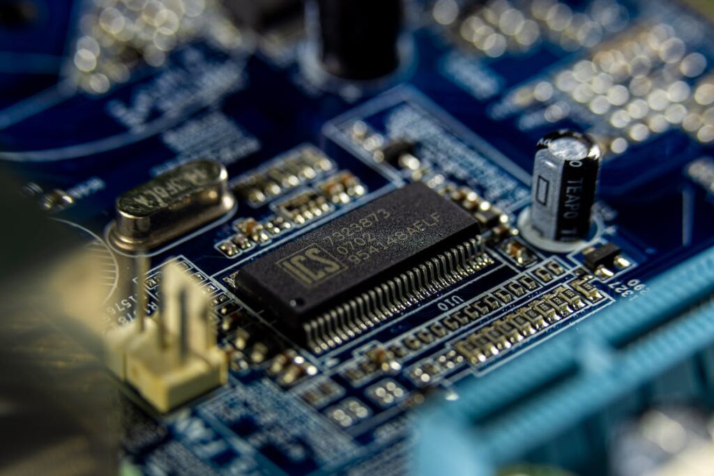
In contrast to a typical circuit board, a high-density interconnector, commonly known as an HDI any-layer printed circuit boards, is a form of printed circuit board that has many interconnections and takes up the least amount of space. To give the circuit board a small and portable appearance, the components on an HDI PCB board are placed close to one another. In the present world, several technical industries, such as the medical, automotive, and military, prefer to embrace and value HDI.
In the PCB and electronics industries, HDI any-layer printed circuit boards are becoming more important. However, to function at a higher level, smaller and lighter electrical components are needed. To accommodate this, you'll need to pack more features into a smaller area. Your success in accomplishing this goal is aided by HDI boards. The characteristics and advantages of such panels are covered in full in this article.
HDI any-layer printed circuit boards have a higher per-unit circuitry density than conventional PCBs. They are produced utilizing a variety of materials, including FR4, metal, fiberglass, etc., according to the intended use. They use hidden and blind vias in addition to microvias, which have a diameter smaller than 0.006 inches. High-density circuit boards have each of the qualities listed below:
We owe the existence of many of the current electronics we use, especially those that have greatly decreased in size and weight in recent years, to HDI technology found on printed circuit boards and other places. Smaller gadgets are more likely to employ HDI technology.
A skilled supplier is required because of the very tight tolerances of high-density connection PCBs. A layout mistake or even a slight defect might have a big effect. Leading HDI printed circuit board supplier Millennium Circuits Limited can provide high-quality boards with a lot more circuitry than your typical PCB.
A high-density interconnector PCB may be categorized into six main types. These six HDI PCB types are:
The advantages of HDI technology over other options might help your project reach its full potential. If you employ the correct design and the proper supplier, HDI boards might improve your product's overall quality and performance, customer satisfaction, and bottom line.
By securing extra components on both sides of the bare PCB using HDI any-layer printed circuit boards, you may cram more capability into a smaller space and raise the equipment's overall capabilities. By using HDI technology, you may make your products more useful while reducing their size and weight.
Reducing component distance and adding transistors improves electrical performance. These qualities improve signal integrity while using less power. Smaller diameters are related to faster signal transmissions, lower overall signal losses, and crossing delays.
Due to their reduced size and fewer layer requirements, HDI boards may be more economical than alternative options since they use fewer raw materials. One HDI board may replace many regular PCBs in a product that previously required several of them. It is possible to attain the same level of usefulness and value while using less space and supplies.
Because HDI technology may minimize the number of components needed in your product, there are several advantages to utilizing less material, including shorter production times and faster time to market. High electrical performance and ease of use make good-density interconnect (HDI) PCBs ideal for testing and troubleshooting.
HDI any-layer printed circuit boards are often created utilizing techniques that are different from those used for other PCB kinds. You should be aware of the following information about the creation of HDI boards and certain design considerations that you should bear in mind:
For multi-layer PCBs, the PCB core and any pre-preg layers are joined using heat and pressure before a sequential lamination layer is added. The needed heat and pressure vary greatly from board to board.
The via-in-pad method
PCBs for high-density interconnects are available in a few different layout options. The most prevalent ones are 1-n-1 PCB and 2-n-2 PCB. It is the "simplest" form of the HDI printed circuit board since it consists of a single build-up of high-density interconnected layers.
The any-layer HDI is another popular choice. For conductors on any given layer of the PCB to readily interface with the laser micro through structures, this requires an unusually thick HDI layout. GPU and CPU processors in smartphones and other mobile devices use these designs.
The next technical development after HDI microvia printed circuit boards uses HDI any-layer printed circuit boards, in which all of the electrical connections between the various layers are made using laser-drilled microvias. The ability for all levels to freely link is this technology's key benefit. AT&S employs laser-drilled microvias that have been copper electroplated to create these circuit boards.
Read more: Custom PCB printing and assembly
The usage of HDI any-layer printed circuit boards is growing every day, particularly in IoT devices, due to their affordability and other advantages. IoT devices are becoming more and more common in manufacturing, warehousing, and other industrial settings as automated industrial equipment advances. Many of these high-tech items include HDI technology. The next technical development after HDI microvia printed circuit boards uses HDI any-layer printed circuit boards, in which all of the electrical connections between the various layers are made using laser-drilled microvias. The ability for all levels to freely link is this technology's key benefit. EuropePCB employs copper-plated laser-drilled microvias to create these circuit boards.
Next: Immersion silver PCB
Do you have any questions, or would you like to speak directly with a representative?