
Contact
Write to Us And We Would Be Happy to Advise You.
Do you have any questions, or would you like to speak directly with a representative?
By ren
In this article, we have prepared a "feast of knowledge" on PCB design and PCB manufacturing. You can read this article to understand the complete process of PCB from design to manufacturing!
The designing process is not an easy one. It's like going from designing a simple prototype of printed circuit boards to a real and functioning one. The kind of rush that one can get when they get off from shaping their dream into reality.
This process is time-consuming and there is a lot of information required before starting it. What are we waiting for? Let's learn about PCB design first and then get back to PCB manufacturing.
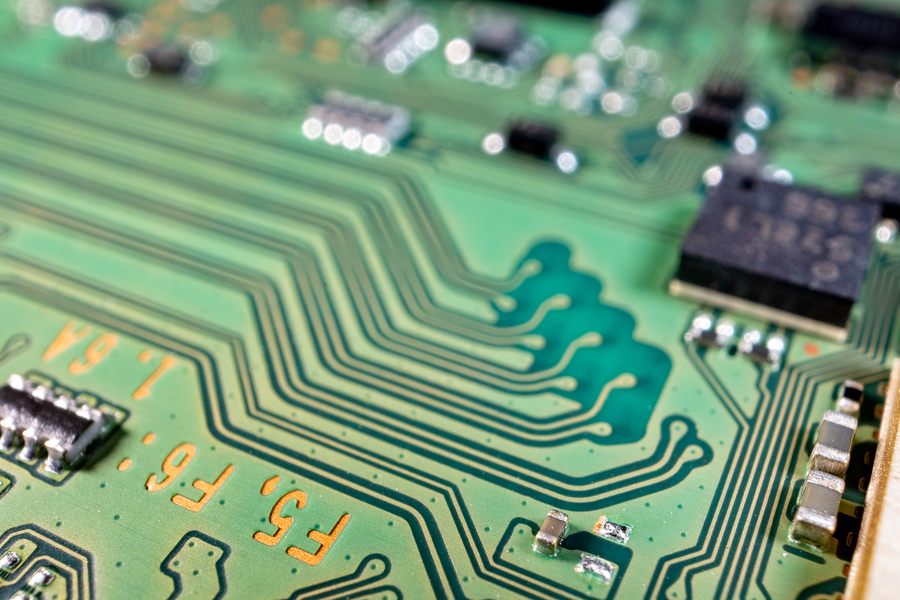
The whole procedure of PCB design is performed in the phase of electrical engineering. At that point, everything is decided on how well the whole design came out to be. Because without the electronics the whole thing is nothing but pieces of metal and plastic.
The steps for the PCB design process start with design and verification. Then it continues and goes through the PCB fabrication process. These steps require technical guidance as it uses computers to ensure everything is done accurately. Because if any mishap happens then it can lead to short circuits as well which is quite dangerous.
All the effort can be lost due to a single mistake. The board lastly goes through complete and very strict testing. If it passes the test the product is then delivered to the customers.
Here is a list that will show how many layers are enough for each product:
The manufacturer will ask you about certain things. Make sure these are correct so that the manufacturer can design them according to your requirements. Following is the information that is required by the manufacturer:
This list of information will be provided by you. Then it’s time for you to wait and watch how your product will be transformed into a new printed circuit board.
As we have learned about printed circuit board design, it’s time to switch to the process of PCB Manufacturing. The whole process of PCB manufacturing is not an easy one. Sometimes the steps of design manufacturing alter. This is because of structural differences.
Sometimes the structures are complex and therefore required more steps while sometimes it goes through an easy procedure. But if any step is cut back even if it was important then it can interfere with the whole performance of the circuit board.
So, make sure to properly implement the steps so the PCB fabrication works the best as it ought to. Let’s discuss the process of PCB manufacturing now. We will cover the whole step-by-step process:
The first step for any circuit designer is the design. A blueprint is made before starting the process. One of the best software that is mostly used is extended Gerber files.
Once the design is decided and encoded on software, it's checked again to make sure there is no error. In the step designing lastly, a proper design for manufacturing DFM is done to ensure that there is enough tolerance.
After the design is made, it is converted into a film using printers. This film will help print PCB circuit boards.
An alkaline solution is prepared to remove unwanted copper. The resistant layer gets removed and then the boards move to the next stage. All the undesirable copper will be removed and the one that is required will stay. It will be protected under the photo-resistant file.
Both the outer and inner layers will need alignment. This way the processing becomes easy. It gets done by an optical punch. This is how the alignment of layers is done.
Once the alignment gets done, it’s time for layering and bonding of the outer layer using substrate molecules. The copper foil is the one that protects the sides of molecules that contain copper which will be used for etching. After they get fused, it leads to bonding.
The next step is drilling. Here manufacturer will drill a hole in the printed circuit board PCB. These holes have small widths and diameters.
With the help of these holes, all the parts are connected. The optical inspection is done to find the perfect spot for drilling. By using computers, every single movement is detected and the process of drilling is done.
The film is subjected to electro-plating in this step. Chemical deposition occurs resulting in the fusion of outer and inner layers. The film goes under a series of processing and as a result, thin copper layers are deposited on its surface and hence Cu gets bored into drilled holes. In this way, holes get covered and this whole process of dipping and depositing is carried out by using computer design software.
After this, the outer layer is imaged and the photo-resistant film is applied to the film and passed to the yellow room as yellow light doesn't have a sufficient wavelength that it would affect the film. Then copper is again deposited on the surface of the film and the outer layer receives this plating. Then it gets further electroplated with tin which allows the leftover copper to be removed. This serves as protecting layer for the film to remain covered during further processing.
In the etching process, the unwanted copper is removed. A process of surface finish is done so all the copper which was in excess is removed. For a good surface finish, chemical solutions are used to remove extra copper. The areas of conducting and connections are made in etching.
In this step, firstly the panels are cleaned. Then by using the epoxy solder mask ink they are covered. The solder mask is applied on both sides of the board. An infused ray of ultraviolet light is blasted through the solder mask photo film.
Surface finish is necessary and cannot be skipped because it makes the product more durable, and long-lasting. It is mostly done using gold or silver.
The second last step for the transformation of the printed circuit board is ink-jetting. Then for a quick turn, the PCB layout or design goes to the last stage i.e. coating and curing.
Lastly, to make sure the product works the best and is made in the best possible way, it gets checked. It is done by electrical test. Once the functionality of the printed circuit board PCB is done, PCB is manufactured.
This is the whole PCB manufacturing process.
We hope that our users have a great idea about the whole process of PCB design and PCB manufacturing. Now that you have understood it clearly, it’s time to find a good manufacturer. What if we tell you a great manufacturer that will make sure your products work the best?
Our suggestion would be to choose Europe PCB to get the best PCB services. The reason we will recommend opting for Europe PCB are as follows:
Do you have any questions, or would you like to speak directly with a representative?