
Contact
Write to Us And We Would Be Happy to Advise You.
Do you have any questions, or would you like to speak directly with a representative?
By ren
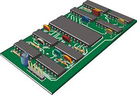
PCB fabrication is the procedure that helps in transforming a circuit board design and then shaping it to a physical structure and all that with addition of specifications that are provided in the design package. Here we will cover the whole process of PCB Fabrication and will guide about the usability of the fabrication process as well.
Raw materials used during the fabrication process includes High strength low alloy steel (HASL) and immersion gold plates and are widely used in PCB industry nowadays. HASL prevent the oxidation on the surface of copper maintaining its properties for processability. Gold plating gives stability and color and also creates flattened coated surface that produces good effect on printed circuit.
Processes:
PCB Fabrication process is an important process since all the working is useless unless we need properly manufacture and fabricat the raw materials.
Let’s discuss PCB manufacturing processes in detail.
The main step for the production is to make its PCB design. There have several software launched to provide us ease and instead of using pen or paper, we can easily make any design with help of a few clicks. Most widely used designing software includes Auto CAD, MAT lab, Eagle, etc. By using this software, you can choose the design of your required. All aspects are properly checked reducing the risk of errors. All the notations according to processing can also be done.
The manufacturer will take the design we have made for export and then approve the production.
After the examination of design, manufacturer convert the design into film with the help of printers that will appear in the production of photo films. These films print pcb circuit boards and they will use these films for imaging PCB. We will obtain a highly detailed and precise PCB design film.
The required product is in the form of plastic sheet electrons on its surface and this appears in form of black ink. This black ink shows conductive parts while another clear portion indicates nonconductive part of PCB. The black portion is the one etched further while the outer layers are clear in the case of copper. Moreover, the printer also develops a coating that serves as protecting a thin layer concerning surrounding. Hence, the film can be stored easily.
To remove unwanted copper, we prepare an alkaline solution. The bare board moves to the next stage as we remove the hard resist layer that needs to cover the copper.This alkaline solution is very powerful and hence removes all the unwanted copper while the desired Cu remains protected under photo-resistant film.
The inner and outer layer require alignments so that processing can become easy. Optical hole punches can do this. Once layers are aligned into one another it is difficult to separate them. Original design in form of file received by printed circuit board manufacturer serves as an example.
In the case of inconsistencies, the screen will display them out, so corrections are easy.
After the alignment, bonding and layering of outer layers with the substrate molecules occurs. This outer layer consists of thin fiber sheet aligned with epoxy resin. Thin Cu foil protects and covers the both sides of substrate molecule that contain elements of Cu for etching. Then they fuse together and form a bond.
Substate molecule attaches with the film before the placement of Cu. Now an Al foil and copper foil form a complete fused surface ready to be pressed.
This stack is heated by applying pressure and then allowed to cool under required conditions. This will cause little unpacking and hence we get the required multi-layer product.
PCB circuit board manufacturer drills holes on the circuit board. These holes have very small width and diameter. All components that are to be connected with it, are linked through these holes. X-ray detector or some optical inspection methods are used to find exact drilling spot. Every small movement of drill is controlled with the help of computers. Such machines use original file design to identify particular drill spots.
After the completion of drilling, additional Cu is removed by using profiling tools.
During this process, the film is subjected to plating. Chemical deposition occurs resulting in the fusion of outer and inner layers. The film goes under a series of processing and as a result, there is a thin layer of Cu deposited on its surface and hence Cu gets bored into drilled holes. In this way, holes get covered and we use computers to carry out this whole process of dipping and depositing.
After this, outer layer is imaged and photo resistant film is applied to the film and passed to yellow room as yellow light don’t have sufficient wavelength that it would effect the film.
Moreover, copper is again deposited on surface of film and outer layer receives this plating. is further electroplated with tin which allows the left over copper to be removed. serves as protecting layer for film to remain covered during further processing.
The final etching process, the high quality tin protects the desired copper in this process. The copper that is unexposed and is not wanted is removed as it goes though the procedure of removal. Then for the surface finish, excess copper is removed by using chemical solutions. Similarly, the material of tin hence protect and keep the quality of copper in good shape. In this process the areas of conducting and connections are made.
In this process of PCB Manufacturing, the next step that comes is the procedure of solder mask. First of all, is cleaning the panels. Then epoxy solder mask ink will cover them, soldermask following on both sides of the board. An infused ray of ultraviolet light is blasted and the process of it is that it passes through the solder mask photo film. At the same time, sometimes the part covered by the outer layer is unchanged, i.e. not hardened, and will eventually undergo the removal process.
To make it a high-quality product, I.e. to make it more durable, chemical plating is done. The chemical plating is done with gold or silver. Some printed circuit board receives the hot air-level pads in this stage which leads to uniform pads. All of this leads to the procedure of surface finish.
The board that was almost completed and is about to be transformed receives ink-jetting. The PCB design finally then passes to the last stage which is the stage of coating and curing.
To make sure everything goes smoothly, for the final part electric tests are being done on PCB. In this process, the functionality of PCB is confirmed making sure that it conforms to the original PCB prototyping.
The question that arises is whether the fabrication process is necessary to understand or not. Because this process is the PCB layout or design process but still there are specifications that should be noted which will be provided and only then the specific design will be made. All of this can only be done if the whole procedure is completely understood by the user so they can question the high qualityPCB o product. Once you fully understand the procedure, you can decide whether to make appropriate choices for outer layers, materials, PCB layout, and optical inspection, etc., as it affects the overall performance of the PCB assembly and its manufacturability.
A good service provider is necessary if you are looking for a high-quality product. Not only the PCB Layout but the whole process of PCB manufacturing is complex and it should be done in a professional environment where there are proper facilities of professional engineering and quick response service as well. We have good news for you because Europe PCB is known to provide the best services and they are known as one of the great service providers of PCB assembly manufacturers all around Europe and provide their services in SMT & DIP and much more.
Why you need a good PCB service provider:
Why Choose Europe PCB:
Do you have any questions, or would you like to speak directly with a representative?