
Contact
Write to Us And We Would Be Happy to Advise You.
Do you have any questions, or would you like to speak directly with a representative?
By hqt
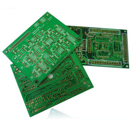
The so-called single board is that on the most basic PCB, designer concentrate all parts on one side, and the wires on the other side. Because the wires only appear on one side, we call this a PCB a Single-sided. Because there are many strict restrictions on the design line ( It is only one side, designer can't cross the wiring though, must rout alone.), so they don’t use it anymore, but they used it more in the early days;
People base mainly the single-board wiring diasgram on network printing. That is, they print a resist on the copper surface. After etching, they print a mark on the solder resist. Finally, punching complete the part guide hole and shape. In addition, some small and diverse products use a photoresist to form patterns. If you custom the Single-side Board, design and layout PCBs is the key.
When starting the PCB layout, you should complete the schematic design. Get a correct schematic, this is the basis of the single-board proofing design. Through the schematic diagram, we can get a netlist of the connection properties of each device. According to the parameters of the device, we can find the relevant component information and establish the package of all components. In addition, requiring the structural parts, the designer need give the dimensions of the plate and frame. As well as the positions of various installation positions and functional excuses.
First, they need to import all package files and netlists into the PCB file with the outer frame established. During the import process, some component packaging errors may appear. Please correct the errors according to the error prompts.
We need to fix components such as LEDs, buttons, card holders, LCDs, infrared emitters, etc. Move these devices to the corresponding installation positions and select lock in the properties to prevent misoperation.
The purpose of the general layout is to determine the position of each functional module. In PCB design, the default is generally:
Except for the devices that need to be mounted on the surface, all the patch devices are placed on one side of the plug-in device, which is generally the bottom layer;
The measuring unit is placed in the lower left corner for easy access to the line;
The MCU is placed on the back of the LCD and the leads are short enough;
The interface part is placed in the lower right corner of the PCB for easy wiring;
Transformers should be far away from magnetic leakage sensitive devices such as transformers and manganese copper shunts;
Keep sufficient creepage distance between circuits that need to be isolated;
Complete the placement of the corresponding device for each functional module. The factors that need to be considered in the local layout are:
The crystal should be as close as possible to the crystal pins, so that the traces are as short as possible;
The decoupling capacitor should rely on the power input pin of the IC as much as possible;
Devices with high-speed connections between ICs should be as close as possible;
It is necessary to consider the convenience of maintenance and optimize the placement of some devices to avoid production difficulties;
Keep a certain board margin, the required margin should be more than 4mm, otherwise the SMT workshop is likely to cause accidental damage to the chip picker during the placement, which will cause the device to collide with the chain during wave soldering, and cannot be used for wave soldering at once Complete the plug-in welding, need to arrange more welding repairs;
Varistors, polyester capacitors, transient suppression diodes, and zener diodes, filter capacitors should be placed at the front end of the device to be protected;
Note the distance between high and low voltage signals.
The wiring of components is also a very important process for PCB single-side Board. Pay attention to the following aspects when wiring:
By understanding the current that each device may flow and the maximum inrush current, you can roughly understand the possible effects of signals carried on the traces on other signals. To set the trace thickness
The traces from the high-voltage signal to the ends of the varistor and polyester capacitor should use a wider line width as much as possible, so that the protection device can timely release the overload energy, and at the same time prevent the line from being burned by the instantaneous high current;
The low-voltage power supply signal main line is routed with 36 mils to reduce the resistance of the wires. A width of 24 mils or less can be used near the chip.
The small signal connection can use 10mil or 12mil. Too thin will lead to too high scrap rate and too thick is meaningless.
Do not run traces near high-frequency signals, such as the bottom of a crystal;
Minimize via connections. The quality of the wiring directly affects the performance. In actual wiring, it may need to be overturned, and even return to the schematic diagram to modify the definition of the IO port. This is the most time consuming part.
The power cables should be routed with sufficient width to avoid sudden changes in line width and right-angle corners. In addition, the power lines cannot be looped.
Forming a large ground plane is equivalent to completing the wiring of the ground wire.
When adjusting, prevent the large piece of ground from being connected to the main ground only through a few vias. Pay attention to the integrity of the ground under the chip. In addition, you can better observe the beautiful layout of the wiring and components, as well as whether the return flow of each signal is complete. At this step, the adjustment and modification of all device labels are completed, and the company logo and PCB version number are marked.
It also points out errors and highlights them.
The export format is Protel PCB 2.8 ASCII File.
Prev: Ceramic PCB
Do you have any questions, or would you like to speak directly with a representative?