
Contact
Write to Us And We Would Be Happy to Advise You.
Do you have any questions, or would you like to speak directly with a representative?
By hqt
A printed circuit board is a dielectric plate, on the surface and/or in the volume of which electrically conductive circuits of an electronic circuit are formed. The printed circuit board is the backbone of any modern amateur radio design and is designed for the electrical and mechanical connection of various electronic components. The electronic components on the printed circuit board are connected by their pins to the elements of the conductive pattern, usually by soldering. The color of the printed circuit board can be any: green (default), blue, red. black, it does not affect other characteristics of the board.
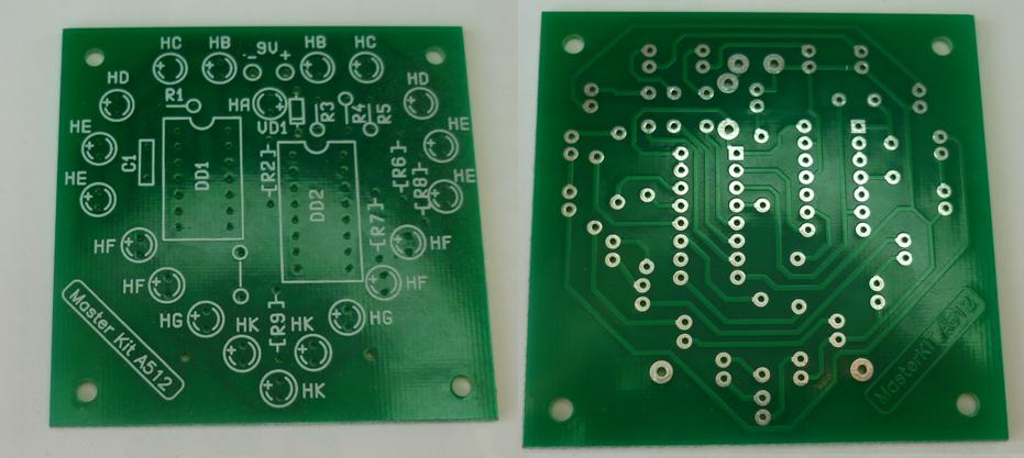
The PCB has two sides. Conventionally, they can be called the front side and the side of the printed conductors. In contrast to surface-mounted mounting, the electrically conductive pattern on the printed circuit board is made of foil, which is entirely located on a solid insulating base. The printed circuit board contains mounting holes and contact pads to which the leads of radio components are soldered. In addition, printed circuit boards have vias for electrically connecting foil sections located on different layers of the board. On the front side, markings are applied (auxiliary drawing and text according to the design documentation) so that you can figure out where and in what polarity to install this or that part.
The pictures below show the same PCB from different sides.
Depending on the number of layers with an electrically conductive pattern, printed circuit boards are divided into:
According to the properties of the base material:
Rigid
Flexible
Printed circuit boards can have their own characteristics in connection with their purpose and requirements for special operating conditions (for example, an extended temperature range) or specific applications (for example, boards for devices operating at high frequencies).
The basis of the printed circuit board is a dielectric; the most commonly used materials are glass fiber laminate, getinax.
Also, the basis of printed circuit boards can be a metal base covered with a dielectric (for example, anodized aluminum), copper foil of the tracks is applied over the dielectric. These printed circuit boards are used in power electronics to efficiently dissipate heat from electronic components. In this case, the metal base of the board is attached to the heatsink.
As a material for printed circuit boards operating in the microwave range and at temperatures up to 260 ° C, fluoroplastic reinforced with fiberglass (for example, FAF-4D) [2] and ceramics are used.
Flexible boards are made from polyimide materials such as kapton.
The conductive paths are usually covered with a layer of insulating varnish (called a "mask"), and only the contact pads are exposed to the mask and ready to be soldered. The contact pads of the vast majority of Master Kit boards are silvery and shiny, as they are covered with a layer of tin, which protects them from premature oxidation during long-term storage. These boards are easily soldered using the most common rosin channel solder, and you do not need to purchase additional rosin or flux.
If you come across a board, the contact pads of which are not covered with a protective tin layer, but copper (characteristic yellow color), then it is necessary to use rosin and flux to remove oxides and high-quality soldering. In advanced cases, grinding the contact pads with fine sandpaper ("zero") helps.
Sometimes there are holes on the printed circuit board for its fastening in the case. If such holes are not provided, you can independently drill them with a conventional drill in a place free from components. Of course, you need to make sure that the new hole does not break any of the printed conductors or bonding pads.
If the printed circuit board barely fits into the housing planned for its placement, the board can be sharpened from the ends with a file. But make sure that the file does not interfere with the conductive paths of the board.
Damaging a PCB is difficult, but if you try, it's still possible. First, do not bend it too much - the board may break! And do not overheat the board when soldering! Although the conductive tracks and foil pads are glued to the base of the board with very high quality glue that is resistant to high temperatures, excessively long continuous exposure (more than a few seconds) to the hot tip of the soldering iron on the contact pad can lead to its separation from the base. If this still happens, you can glue the torn off track. If the track is not just peeled off, but torn off, a piece of wire can be used to restore the integrity of the electrical circuit.
You can rinse the printed circuit board from the remnants of soldering materials using an alcohol solution (alcohol).
Do you have any questions, or would you like to speak directly with a representative?