Prototype circuit board assembly

09 Sep, 2022

By ren

Influence of Prototype circuit board assembly on PCB manufacturing

Making PCBs is a difficult process. As a result, it's critical to avoid certain production mistakes. A critical phase of PCB production is PCB prototyping. Also, the PCB prototype board gives a lot of benefits. PCB makers look for methods to save expenses and wait times. Prototype circuit board assembly lowers the cost of production. This is because it enables producers to find any flaws before a board is fully produced.

Before making a printed circuit board in bulk, PCB producers must prototype the device. A proof of concept involves also Prototype circuit board assembly. It displays a product to potential customers and investors while proving the intellectual property.
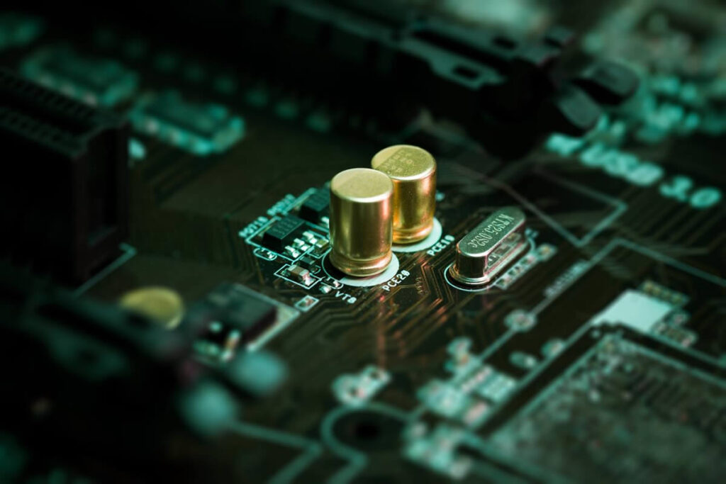
Prototype circuit board assembly

A PCB prototype: what is it?

Prototype circuit board assembly is essential to the process. It is a preliminary sample intended for PCB design functionality testing. The majority of prototypes are created specially to evaluate a board's performance and usefulness. Manufacturers of PCBs create a prototype before creating the final product.

• Various prototype kinds are used by engineers and designers to test different design elements. Before beginning the full-scale fabrication of boards, a prototype is necessary. As a result, it acts as the first circuit board sample. From the conception of the design to the completed product, prototyping a board is essential. You may evaluate a design's functioning using prototypes.

• With prototypes, you may repair and debug any circuit board fault. Prototype PCBs are also perfect before mass manufacture. Mass manufacturing without a prototype is never without danger. Even a little error in the production of a board may be quite expensive. Additionally, fixing such a mistake could take some time.

• Soldering might be exceedingly challenging if there is a flaw in the PCB design. Additionally, it is more difficult to find board flaws without a prototype. Prototypes are made before the mass manufacture of the boards to avoid any potential loss or danger. PCB prototype and full spec manufacturing projects are two different things. Only after a prototype has demonstrated its usability can full-spec production start.

Prototype Board Types

Circuit board prototypes of many kinds may be used by designers to test various design elements. The durability of a circuit board is not there in a prototype. So, before mass manufacturing, this prototype enables designers to test circuit boards.

You may experiment with other circuit designs if you make a mistake with a prototype. You may go on to the next step of manufacturing after the circuit is operating as required.

Preboard

This particular prototype circuit board uses the "pad per hole" construction method. This shows that on the circuit board, each hole is electrically isolated. Therefore, soldering is the only way to connect components. Perforated boards are very durable. Additionally, because preboards may create connections as they like, they provide greater design freedom.

Breadboard

This circuit board doesn't need solder. Small holes on a breadboard may accommodate electronic components. These holes are neatly set out in rows and columns. Additionally, the breadboard's columns make it simple to construct a circuit without the need for wires. One of the terminals may be inserted into the other holes in the same column. A breadboard also enables you to organize circuit boards in various ways.

Veroboard

An example of a prototype circuit board is this. It consists of copper strips running vertically through a grid of holes. Wires are replaced with connections between the holes. They thereby make it simple for components to link to one another. Additionally, soldering is needed for several of the connectors on the Vero-board. Vero-boards are more compact and allow for more efficient circuit design.

Process for Manufacturing PCB Prototypes

They are a staple of contemporary technology and essential to various electronics and other electrical components.

  • The prototype phase is equally crucial to the production process in terms of significance. Prototyping is a procedure that comes before production and is a common industrial practice everywhere.
  • To start, having a basic understanding of prototyping would be quite beneficial.
  • PCB designs are prototyped by manufacturing real samples from schematics and blueprints.
  • Before PCB mass production, it is checked to determine if any tweaks are needed.
  • It's done to ensure there are no design errors or other difficulties when the PCBs are utilized as intended.
  • The bullet points below provide a collection of some of the most important information concerning the PCB prototyping process.

Style

  • Among Designing a PCB prototype style is one of the initial tasks in the production process.
  • At this phase, the PCBs' fundamental design is developed and carefully examined for any conceivable advancements.
  • After the drawings have been finalised, they are sent to an outside source for verification, providing a valuable second opinion.

A list of the materials

  • The phrase "Bill of Materials" refers to every material that would be needed to manufacture a PCB.
  • Consider it as an electronic equivalent of the "ingredients" required to make the finished dish.

Routing Diagrams

  • This phase includes the routing design or production of the traces that link the different PCB components.
  • Several things to consider, including but not limited to power levels, signal noise production, noise sensitivity, and other factors, must be taken into consideration at this point.

Checks for Design

  • Design inspections are more of a routine procedure than a one-time event.
  • There is a chance that the functionality will be added later owing to a variety of factors, given that each step of the design process adds another layer of complexity.
  • To avoid any possible flaws in the future, it is important to make sure that proper design checks are carried out at every stage of the process.

Making of photos and film

  • A photo film is made from the design schematics and will be used to construct the final PCB prototypes.
  • It will highlight the portions of the circuit board that are composed of conductive copper layers and those that are not.

Inner Layer Printing

  • In inner layer printing, the substrate material receives copper.
  • It hardens, leaving a covering that identifies the board's soft copper circuitry.

Layer Alignment and Fusing

  • If more layers are to be added to the final board design, this is relevant.
  • After the boards are correctly aligned, the assemblies are fused.

Hole Drilling

  • Whether utilizing mechanical or laser drills, this is the stage when holes are drilled in the circuit boards for the insertion of vias.
  • It is a common procedure that occurs in all significant PCB designs, regardless of the intended use.

Copper plating

  • The copper plating step, which offers the primary layer to build up and develop the circuitry, is where the circuits of the board get started.
  • The actual procedure is electroplating, in which a thin coating of copper is applied to the board and any extra is removed by etching. The plating step often occurs

The last engraving

  • The removal of extra layers of metallic deposits by chemical solutions is more comparable to erosion than anything else during the last stage of the etching process.
  • The final products then serve as the foundation for future design work, such as the arrangement of different components.

Application of the solder mask and surface finish

  • The PCBs are then covered with a layer of solder mask as a protective layer to stop the copper traces from oxidizing.
  • For a similar reason, a layer of finish is also applied; it is often composed of silver or gold and assists the solder to flow correctly throughout the PCB's surface, producing superior results.

Silkscreen printing and cutting

  • Important board information is included during the silkscreen application step.
  • The cutting step comes after the stage, in which the smaller chips are separated from the bigger board and ready for testing and other uses.

Testing and evaluation

  • The phase when testing and assessment take place is last but by no means least.
  • The finished PCB prototype must be tested for functionality, design flaws, enhancement opportunities, and other aspects. The firm doing the prototyping, a third party, one's expertise, or one's experts may perform the real testing and assessment.
  • The final design typically falls short of expectations. To get the intended outcomes, it might include anything from making modest tweaks to completely redesigning the PCB layouts.

Read more: PCB Assembly Prototype Manufacturing Sevice 2023

Conclusion

PCBs, or printed circuit boards, are the foundation of all significant electronics. Nearly every computational electronic gadget incorporates these amazing achievements, including basic ones like digital clocks and calculators. For those without technical knowledge, a PCB is a circuit board that transmits electrical impulses via electronics to meet the device's electrical and mechanical circuit needs. In other words, PCBs direct the flow of electricity, which activates your electronics. If you are looking for Prototype circuit board assembly services, you can visit EuropePCB. They provide great deal services.

Contact

Write to Us And We Would Be Happy to Advise You.

    l have read and understood the privacy policy

    Do you have any questions, or would you like to speak directly with a representative?