
Contact
Write to Us And We Would Be Happy to Advise You.
Do you have any questions, or would you like to speak directly with a representative?
By hqt
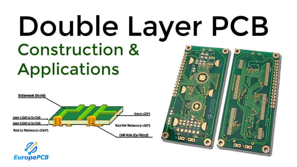
A 2 layer PCB is a printed circuit board that has two copper layers. The copper layers are separated by a thin layer of dielectric material. The dielectric layer can be made of different materials, but the most common is FR-4.
2 layer PCBs are the most common type of PCBs. They are used in a wide variety of electronic devices, from cell phones to computers.
2 layer PCBs are made by bonding two pieces of copper together. The copper is then etched to create the desired circuit. The circuit is then covered with a thin layer of dielectric material.
2 layer PCBs have a number of advantages over other types of PCBs. They are cheaper to manufacture, and they can be made smaller and lighter. They are also easier to repair.
If you are looking for a PCB manufacturer, there are a few things you should keep in mind. The first is the size of the PCB. The second is the complexity of the circuit. The third is the number of layers.
When it comes to size, the smaller the better. The smaller the PCB, the cheaper it is to manufacture. The smaller the PCB, the easier it is to work with.
The complexity of the circuit is also an important factor. If the circuit is simple, it can be made on a single-layer PCB. If the circuit is complex, it will need to be made on a multilayer PCB.
The number of layers is also an important factor. The more layers a PCB has, the more expensive it is to manufacture.
2 layer PCBs are the most common type of PCBs. They are used in a wide variety of electronic devices, from cell phones to computers. If you are looking for a PCB manufacturer, there are a few things you should keep in mind. The first is the size of the PCB. The second is the complexity of the circuit. The third is the number of layers.
2-Layer PCB Manufacturing refers to the process of creating a two-layer printed circuit board. This type of PCB is typically used for low-density applications such as consumer electronics. The manufacturing process begins with a copper-clad laminate, which is a sheet of copper bonded to a substrate. This laminate is then drilled and etched to create the desired circuit pattern. The next step is to apply a solder mask, which is a protective coating that helps to prevent shorts and soldering. Finally, the PCB is finished with a silkscreen legend that indicates the component locations and other important information.
Prototyping is the process of creating a physical model of a product or design. It is often used to test the feasibility of a design or to create a working model of a product before it is mass-produced.
There are two main types of prototyping: additive and subtractive. Additive prototyping, also known as 3D printing, creates a three-dimensional model of a product or design using a printer. Subtractive prototyping, on the other hand, involves machining or carving a product or design from a block of material.
Both additive and subtractive prototyping have their advantages and disadvantages. Additive prototyping is typically faster and less expensive than subtractive prototyping, but it can be less accurate. Subtractive prototyping is usually more accurate, but it is often more time-consuming and expensive.
Which type of prototyping you choose will depend on your specific needs and goals. If you need a quick and dirty prototype, additive prototyping may be the way to go. If you need a more accurate prototype, subtractive prototyping may be the better option.
PCB Assembly is the process of connecting electronic components to a printed circuit board (PCB) to create an electronic device. The components are typically soldered to the PCB using surface-mount technology (SMT) or through-hole technology (THT).
PCB assembly can be done by hand, using manual soldering techniques, or by using automated assembly machines. The assembly process typically starts with the placement of components on the PCB using a pick-and-place machine. The components are then soldered to the PCB using a solder paste and a reflow oven.
After the soldering process is complete, the PCB is typically inspected for defects using a microscope. Defective PCBs are repaired or scrapped.
The PCB assembly process can be complex and requires a high degree of accuracy and precision. It is important to carefully select the assembly process and components to ensure that the finished product meets all performance and quality requirements.
2 Layer PCB Manufacturing refers to the process of creating a two-layer printed circuit board. This type of PCB is made up of two conductive layers separated by an insulating layer. The conductive layers are typically made of copper, and the insulating layer is made of a material called FR-4. 2 Layer PCBs are commonly used in a wide variety of electronic devices, including computers, cell phones, and home appliances.
The manufacturing process of a 2 Layer PCB starts with the preparation of the copper foil. The foil is then etched to create the desired circuit pattern. Next, the foil is laminated to the FR-4 insulating layer. After the laminate is cooled, it is drilled to create the holes for the through-holes. Finally, the circuit board is plated with a thin layer of copper to provide protection and to give it a finished look.
Soldering is a process in which two or more metal surfaces are joined together by melting and flowing a filler metal (solder) onto the joint. The filler metal has a lower melting temperature than the base metals being joined, so it can be melted and drawn into the joint by capillary action.
In order for the solder to properly wet the surfaces to be joined, they must be clean and free of oxides. The soldering process usually starts with cleaning the surfaces to be soldered. This can be done with a number of methods, including chemical cleaning, mechanical abrasion, or a combination of both.
Once the surfaces are clean, a flux is applied to help the solder flow evenly into the joint and to prevent oxidation of the metals. The flux also helps to remove any oxides that may have formed during the cleaning process.
The joint to be soldered is then heated, usually with a soldering iron, until the solder melts and flows into the joint. The joint is then allowed to cool, and the solder will solidify, creating a strong bond between the two surfaces.
There are a number of different types of solder available, and the type of solder used will depend on the application. The most common type of solder is a lead-tin solder, which is used for electrical and electronic applications. Lead-free solders are also available for use in applications where lead is not desired.
In order to make a 2 layer PCB, there are several process steps involved. The first step is to create the circuit board layout. This can be done using a CAD program. Once the layout is complete, the next step is to print the circuit board onto a special film. The film is then placed onto a copper-clad board and exposed to UV light. This process creates a negative of the circuit board layout onto the copper-clad board.
The next step is to develop the copper-clad board. This is done by placing the board into a special solution that etches away the exposed copper. Once the etching is complete, the board is then cleaned and ready for the next step.
The next step is to apply a thin layer of copper onto the exposed areas of the board. This is done using a process called electroplating. Once the copper has been applied, the board is then ready for the soldering process.
The final step is to solder the components onto the board. This is done using a soldering iron and solder. Once the components are in place, the board is then tested to ensure that it is functioning correctly.
As the name suggests, Quality Control is a process that is used to ensure that a product or service meets the required standards before it is released to the customer. In the case of 2 layer PCB manufacturing, Quality Control is essential in order to ensure that the final product is of the highest possible quality and will function correctly.
There are a number of steps involved in Quality Control for 2-layer PCB manufacturing, which include incoming inspection of all materials, in-process inspection of the PCBs as they are being manufactured, and final inspection of the completed PCBs.
Incoming inspection is important in order to ensure that all of the materials that will be used in the manufacturing process meet the required standards. This includes checking the quality of the raw materials, such as the copper sheets and the adhesive used to bond the layers of the PCB together.
In-process inspection is carried out at various stages of the manufacturing process, in order to check that the PCBs are being manufactured to the correct specifications. This includes checking the thickness of the copper sheets, the width of the traces, and the overall dimensions of the PCB.
A final inspection is carried out once the PCBs have been completed, in order to check that they meet the required standards. This includes checking for any defects, such as short circuits, open circuits, or incorrect component placement.
Quality Control is an essential part of 2 layer PCB manufacturing, in order to ensure that the final product is of the highest possible quality. By carrying out incoming inspection, in-process inspection, and final inspection, it is possible to identify and rectify any issues that may occur during the manufacturing process, before the PCBs are released to the customer.
There are several methods of shipping a 2 layer PCB. The most common is to use a flat rate shipping service such as UPS or FedEx. This is the most economical way to ship a 2 layer PCB. Another option is to use a local company that specializes in shipping PCBs. This option is often more expensive, but it can be faster and more reliable. The last option is to use a freight service. This is the most expensive option, but it is the most reliable.
After-sales service is the public service provided by a company to customers who have purchased its products. It is a part of customer service that deals with the provision of support to customers after they have purchased a product. The after-sales service includes any type of support provided to the customer after the product has been purchased, such as warranty service, repairs, and product returns.
The aim of after-sales service is to ensure that the customer is satisfied with the product they have purchased and to provide them with assistance if they have any problems with it. After-sales service is important for building and maintaining customer relationships, as it can help to increase customer loyalty and encourage repeat purchases.
Companies that provide good after-sales service can benefit from increased sales, as customers are more likely to buy from businesses that they know will offer them support if they have any problems. It can also help to reduce the number of product returns, as customers are more likely to attempt to fix a problem themselves if they know they can rely on the company for assistance.
In order to provide good after-sales service, companies need to have a system in place for dealing with customer inquiries and complaints. They should also make sure that they have trained staff who are able to deal with customer queries effectively. Good after-sales service can be time-consuming and costly, but it is an important part of running a successful business.
Prev: Immersion silver PCB
Do you have any questions, or would you like to speak directly with a representative?