
Contact
Write to Us And We Would Be Happy to Advise You.
Do you have any questions, or would you like to speak directly with a representative?
By ren
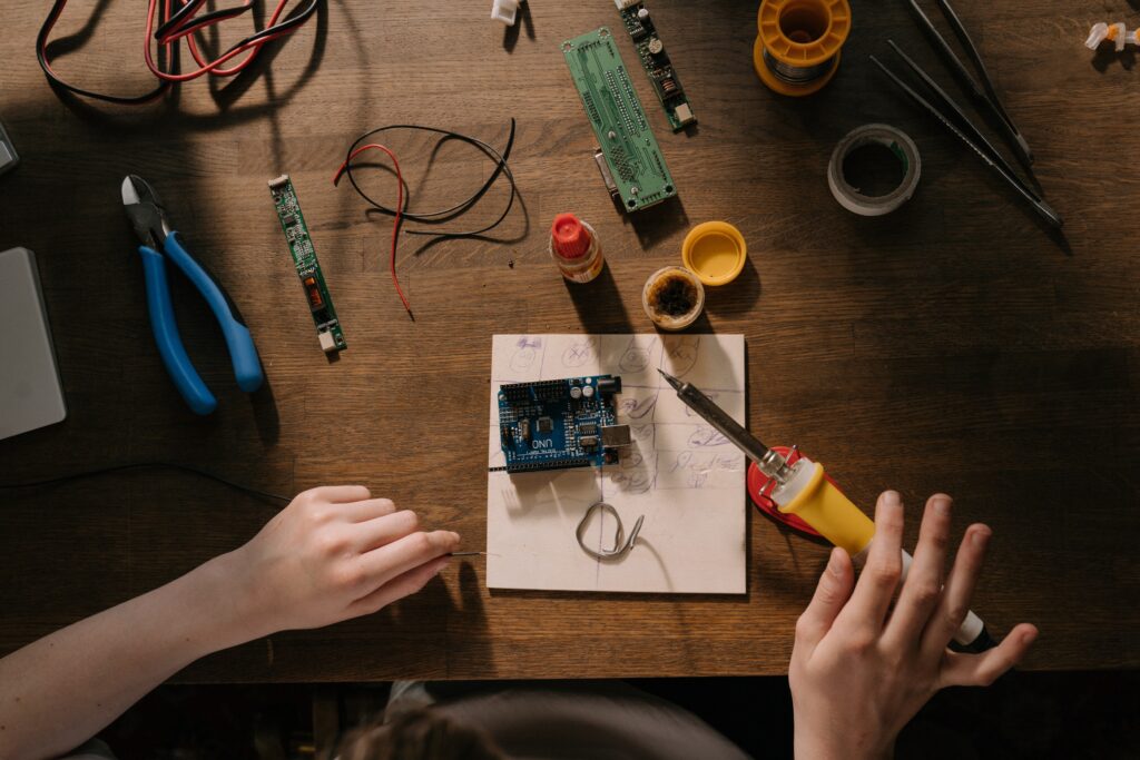
The entire manufacturing process is complex and is influenced by several variables. There could be hundreds of constituents and thousands of solder linkages on a single board, and without proper verification, the entire process is hit or miss. As a result, the electronics manufacturing sector and product developers respond to this difficulty by adopting Circuit Board Assembly Functional Testing techniques to ensure product quality.
Testing can aid in the early detection of critical faults, increasing yield and lowering costs while also improving overall quality and safety. PCB functional testing is one of the most effective and versatile methods for ensuring that a board is ready for use in the real world. Still, it is only one of several testing methods available to a manufacturer.
Choosing the optimal test technique for your scenario and budget can be challenging because each testing method has pros and downsides. We'll go through seven of the most prevalent printed circuit board assembly testing methods in this article.
is done at the end of the manufacturing process as a last quality control operation. In a nutshell, it assures that the device under test (DUT) functions correctly.
Circuit Board Assembly Functional Testing can range from a basic on-off power test to a complete functional examination with tight protocols and testing tools, depending on the complexity of the design and the individual testing requirements.
Circuit Board Assembly Functional Testing can replace more expensive testing processes because of its flexibility. Circuit Board Assembly Functional Testing is more direct than other testing approaches since it simulates the natural working environment.
However, determining the reason for any faults may be more complex, and functional testing may miss boards that fail early in the product's lifecycle, unlike burn-in testing.
With small-batch manufacturing, complete 100 percent functional test emulates being done to assure that every board leaving the production line is functioning.
Highly customizable and adaptable. It is possible to test almost every sort of PCB.
Other testing methods that require specialist equipment are more expensive and inconvenient.
Stage: Following PCB construction and before aging/burn-in testing
Suitable for: PCBs in batches
Advantage: All end-product or PCB behaviors are covered.
It is the final stage of a PCB assembly's testing. The Circuit Board Assembly Functional Testing machine simulates the actual behavior of the PCB and evaluates whether it is a pass or fail. Test probes, connection cables, power supply, and software make up the functional testing bench. In-circuit testing (ICT) does not address PCB behaviors, but functional test fixtures do.
For example, a mobile PCB or a PC motherboard's bios boot-up followed by a Built-in-self test (BIST). Following the functional testing, the manufacturer is confident enough in the product to provide a warranty for a length of time during which the product has proven to be durable.
The functionality tests of a PCB assembly in a specific PCB domain usually do not vary with each version. It only differs somewhat from generation to generation. Because the basic functionalities remain the same throughout generations, PC motherboard functionality test devices may test different motherboards with different revisions.
Some unique tests focus on the products or PCB's behavior in the end-user environment and the previous functional testing. These can differ significantly depending on the PCB and end product.
Some frequent testing is IP rating tests, drop tests, water resistance tests, voltage surge tests, electromagnetic interference (EMI) tests, and radio-frequency interference (RFI) tests.
Any mass-produced electronic item will almost certainly have a PCB that has undergone stringent testing procedures. These PCB assembly testing processes are intended to detect and avoid PCB manufacturing flaws, faulty components, soldering issues, functionality difficulties, component alignment issues, and quality concerns, ensuring that the end product lasts as long.
Let's look at a variety of PCB assembly test methods right now!
PCB testing can be done in various ways, depending on their complexity. The most common methods for testing PCBAs during the assembly process are discussed here.
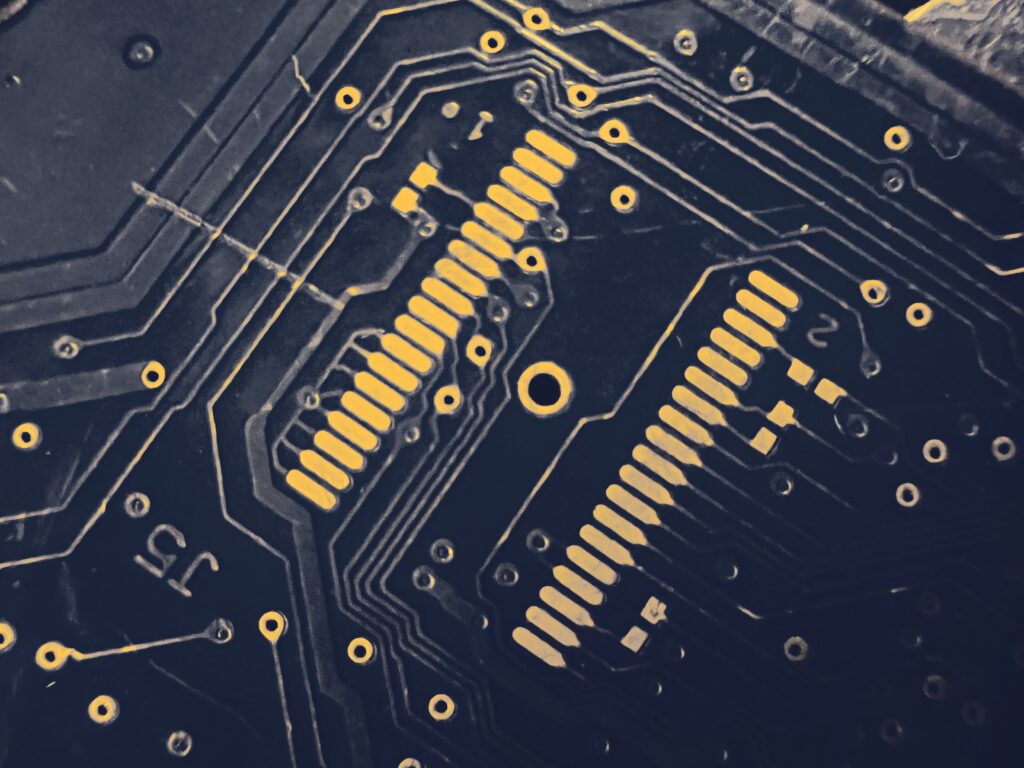
In-circuit testing (ICT) combines several separate testing devices into a single device. Test probes connect to test points on the PCB, which connect the test system to the PCB. Circuits and components are electrically tested against critical values.
The most prevalent defects that ICT may detect are solder shorts, missing components, component failures, raised pins, component shifts, and poor soldering.
Open circuit tests, short circuit testing, resistance measurement, capacitance measurement, inductance measurement, diode of current measurement, and voltage level measurements are all standard electrical measurements made by ICT probes.
The regular bed of nails test and the flying probe test are the two tests available for in-circuit testing.
Suitable for: Except for newer densely packed boards, PCBs are suitable.
Advantages: 85-98 percent; ability to execute several parallel test measurements at once.
Disadvantages: Equipment cost; difficulties updating nail beds
Fixtures connect the assembled PCB to the tester in in-circuit testing machines. A fixture is made up of probes (needles) that are related to specified test sites on a PCB. Fixture wires link the probes to the fixture interface pins. These cables allow you to swap out probes for different PCB test sites.
The interface pins on the fixture are connected to the interface pins on the tester module. Through this interface, the tester sends various signals to the PCB and receives signals back. To detect any anomalies, the tester compares the received signals from the PCB to standard signals for the specified PCB.
Machines for in-circuit testing are available. Because the device cannot access test spots on new densely packed PCBs, and because PCBs are becoming increasingly complex, this method is becoming less and less popular.
Advantages: Benefits include eliminating the need for test fixtures for each PCB version.
Disadvantage: A longer test cycle time is a disadvantage.
Flying probe testing is an in-circuit test system that conducts tests using two or more probes that can move across the PCB board and lower probes on test pads. It performs tests in sequential order. This method may test high-density PCBs, PCBs that don't fit into average ICT test rigs, and PCBs with remote connections with a test pitch of 0.2mm.
Stage: in SMT assembly, following reflow soldering
Suitable for: All PCBs, regardless of volume
Advantages: Speedy and precise
Disadvantages: only test the assembly's surface
This method employs numerous cameras or microscopes to obtain photos of the PCB assembly. With software, the images are then compared against reference images.
This method can also test the end product's quality and visually record the PCB assembly process. The automated Optical Testing method, which is more precise and faster than human visual examination, substitutes human visual inspection.
Missing components, misplacement, misalignment, overall quality, and PCB assembly measurements are all common problems detected with AOI.
This method, commonly known as the boundary-scan method, is a debugging method for integrated circuits (IC). A JTAG interface port on PCBs that support boundary-scan allows access to ICs and embedded circuitry.
Each boundary-scan compatible device includes a shift register for JTAG testing. There is a boundary-scan cell adjacent to each I/O pin of the IC in these devices. Data is sent together with these cells when in shift register mode.
For this test data to enter and exit, each JTAG compatible IC has pre-defined exit and entrance points. As a result, several JTAG compatible components can be tested in a chain. These border scan cells have little effect under normal operating conditions.
The JTAG boundary scan can even monitor the returned data from the shift register chain while in test mode to verify whether the PCB assembly has passed the JTAG test.
Suitable for: PCB fabrication in batches
Advantage: Extremely dependable, mainly when repairing PCBs.
Disadvantage: A complex setup is a disadvantage.
It is a mechanism that enables the PCB assembly to perform self-testing. Built-in self-test systems provide high-reliability checks during manufacturing, but they can also assist at later stages, such as when a PCB is repaired, by pointing out where the problem is.
By decreasing the test cycle duration and having a complicated configuration of In-circuit testing (testing with probes) approaches, BIST systems reduce the complexity of PCB assembly testing.
Stage: Following the completion of the PCB assembly
Advantage: It encourages real-world PCBA use over long periods.
Disadvantages: Depending on the needs, it can take a long time.
This testing technique is used to ensure the PCBs' durability and survivability under the most extreme pressures and loads. Burn-In Testing can be an adverse test for the parts being examined because it detects early faults.
During burn-in testing, the electronics on the PCB are continually powered up to maximum rating, depending on the manufacturer's standards. When a board fails at this point, it is referred to as "infant mortality." It is a standard test for PCBs used in military and medical applications.
Before reflow soldering in SMT assembly, an X-ray inspection (AXI) is performed.
Applicable to: BGA PCB
Advantage: Accurate detection of internal flaws
It is a type of examination that looks for faults that aren't visible to Automated Optical Inspection methods. AXI is used to verify solder connections beneath ball grid array (BGA) packages with solder joints underneath the chip packaging. X-ray Inspection is more commonly done on a selected sample basis in the manufacturing process. It differs from solder float test.
This method is also used to inspect silicon wafers for internal defects. AXI is available both as 2D and 3D tests. Generally, this method is considered a costly PCB assembly testing method.
This Circuit Board Assembly Functional Testing article depicts every PCBA testing in the electronics industry. We are sure you should familiarize yourself with PCBA testing at this point. If you're looking for thoroughly tested PCB assemblies, Europepcb is the place to go. High-quality PCBAs and final goods are on your way, and they'll arrive quickly!
Read more: What You Need to Understand About PCB Stencils?
Do you have any questions, or would you like to speak directly with a representative?