
Contact
Write to Us And We Would Be Happy to Advise You.
Do you have any questions, or would you like to speak directly with a representative?
By ren
PCB assembly testing is a sort of testing that occurs after the electrical components specified in a PCB's Bill Of Materials (BOM) are installed onboard. ICT and PCB assembly testing are inextricably connected. Continue reading to learn about the PCB Assembly testing service.
Typically, testing is done on a level surface with a bed of nails and access to many components linked to the PCB. The board may or may not be powered, depending on the type of testing done. A PCB's Bill Of Materials (BOM) is placed aboard. There are two methods for testing PCB assembly:
Onboard testing of a single component/module and investigating its relationship with all other components in the electrical components/modules network. This test is frequently carried out on individual members before being extended to every other element in the network that has a common interest with the examined component.
Testing is done by taking a sample of a few critical components on the circuit and comparing the results of the element (s) to the predicted results.
Power defects, such as shorts or incomplete circuits, are checked over the entire circuit board. The test also determines whether a prototype has any problematic components.
Power-up tests are also included in this form of testing, which significantly reduces a customer's debug demands.
It can identify almost all types of flaws on a PCB. It has a PCB testing platform that is not dependent on the operating system. The testing is carried out under international IPC standards.
In-Circuit Test is one of the most effective and comprehensive implementations for PCBs. ICT equipment practices a panel-bed of nails (test probes) to admit circuit rebuffs on a board assembly and extent constituents individually.
One element at a time, regardless of whether or not they are electrically coupled to other parts. Resistance, capacitance, inductance, analog component operation, and various digital circuit functions can all be measured. Because of the complexity of digital circuits, complete testing may be too expensive. Still, ICT may be valuable for ensuring that printed circuit boards are created correctly and will work as expected.
Each component is measured individually by ICT equipment to ensure it is in the correct location and has a valid value. Because most assembly faults are caused by manufacturing flaws like shorts, openings, or faulty parts, ICT can detect the majority, if not all, of these issues. Static damage is a common cause of IC failure. These errors can also be discovered using ICT. Some testers can also evaluate the functionality of ICs for added assurance.
A matrix of sensors and divers test strategy is required to set up and make extents in a tester system. It can be applied to a wide range of board designs.
A fixture is an interface between the ICT system connector and a fixture. It is a specially constructed interface between ICT and the tested unit. It uses spring-loaded test pins to route the links for the sensor diver points to the appropriate spots on the device in test. It is a one-of-a-kind unit for each assembly that has been tested.
Each board type to be tested has its software. It is in charge of the PCB Assembly testing service system, defining the points to be tested and the value ranges for pass/fail criteria. Each assembly design to be tested has its own set of software.
ICT systems are costly to buy and have an extraordinary cost of ownership. As a result, they're frequently employed on high-volume, high-value assembly.
In practice, 100 percent coverage test is not attainable due to the following factors:
However, when capacity is an issue, "implied testing" may be employed to achieve some confidence. Using this technique, large parts of a circuit, including several components, are examined as a single unit.
Detect manufacturing flaws easily, such as:
Using files from PCB layout software, it's simple to program.
Because the system identifies the node and problem description, there should be no need for further troubleshooting or diagnostic.
ICT does not functionally analyze the circuit assembly and cannot warranty that it will perform adequately. Instead, once the design has been proven correct, it may be utilized to verify that the assembly was completed correctly.
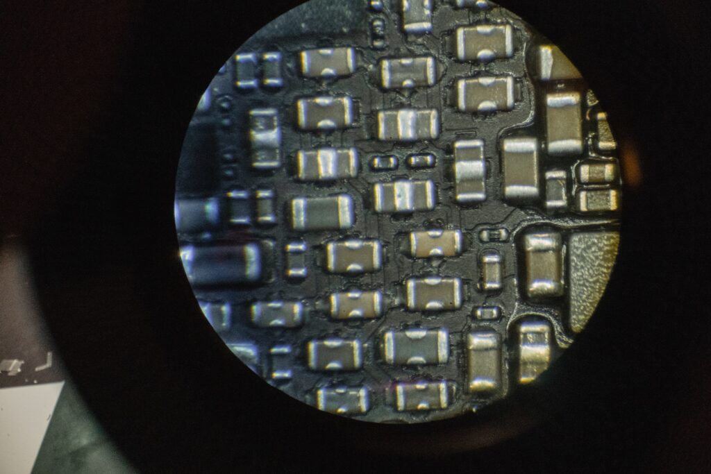
The proper operation of every electronic testing equipment requires high-quality, defect-free printed circuit boards (PCBs). Even though PCB production is mainly automated, some of these boards may contain manufacturing flaws. If left unaddressed, manufacturing defects can result in device failure, product recalls, and a loss of money and time.
To avoid this, PCBs are examined using a variety of procedures at each stage of production. After the visual and AOI inspections have been completed, a functional test (FCT) is the sort of PCB testing done in the final stage of manufacturing. It provides information about the PCB's quality and aids in detecting manufacturing flaws such as missing components, shorts, openings, and incorrect component placements, among other things.
After the successful test during the final test, PCBA inspection with the appropriate electrical safety tests is carried out.
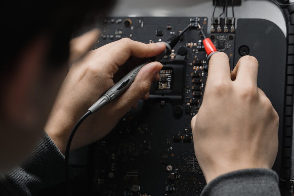
It practices a trial fixture to access many test sites on the PCB's bottom side. In-circuit testing (ICT) is generally utilized on mature devices. ICT can transport test signals into and out of PCBs at high speeds to do component and circuit evaluations if there are enough access points.
A traditional electronic test fixture is a bed of nails tester. It has several pins connected to a measuring device and aligned with tooling pins to contact test locations on a printed circuit board. Several small, spring-loaded pogo pins touch one node in the circuitry of the thing being examined in these devices (DUT).
By pressing the DUT against the nail bed, reliable contact with hundreds, if not thousands, of individual test locations within the DUT's circuitry can be quickly established. The sharp points of the pogo pins used in the fixture may leave a small mark or dimple on devices that have been tested on a bed of nails tester.
ICT offers customers the following benefits:
Printed circuit board assembly is a complicated procedure with the potential for errors. PCB assembly errors are failures in SMT equipment and erroneous component placement.
As a result, a thorough PCB Assembly testing service and inspection are required to ensure that only the highest-quality PCBs are given to the client.
To avoid rework, we place a premium on rigorous quality control. It enables us to reduce overall product prices while also ensuring effective resource management. Extensive PCB Assembly testing service and inspection procedures are implemented throughout the PCB assembly process to detect faults early, ensuring high product quality.
Our broad testing capabilities are ideal for even the most demanding PCB assembly needs. We develop appropriate testing procedures according to the product design, component selection, and batch volume. The following are some of the highlights of extensive PCB Assembly testing service abilities:
For PCB assembly, we use the most advanced testing and inspection equipment, which includes:
It has the following features:
Read more: The Far-Reaching Guide to Circuit Board Assembly
PCB Assembly testing service (& Test Services) is usually performed following a mix of safety and function tests. These extra functionalities can be added to our test devices using simple modules.
Do you have any questions, or would you like to speak directly with a representative?