
Contact
Write to Us And We Would Be Happy to Advise You.
Do you have any questions, or would you like to speak directly with a representative?
By ren
PCB often referred to as Printed circuit boards, is a popular English acronym. It's also referred to as a "printed" circuit board as it's created utilizing electrical printing techniques.
While most individuals encounter printed circuit boards, they immediately know them. These are little green chips with line and copper traces that are found inside the guts of electrical equipment. These boards are bonded together along with epoxy and shielded with insulation material and are manufactured using fiberglass, copper layer, as well as other metal parts. This soldering mask is responsible for the distinctive green hue.
A layout document is often checked for possible errors before Pcb assembly could start so that they may be remedied. A layout for constructability test, or DFM inspection, is a pre-production layout examination that ensures any concerns are rectified well in preparation. This is done to see whether any of the design aspects may cause problems even during the manufacturing process.
For example, with the drive toward minimization, element space can sometimes be too close together, resulting in short and faulty components. A DFM analysis can eliminate these flaws from being a difficulty during the manufacturing process, saving time and money by avoiding the wastage of boards that just don't work. And save expense, inconsistencies and defective elements can be remedied.
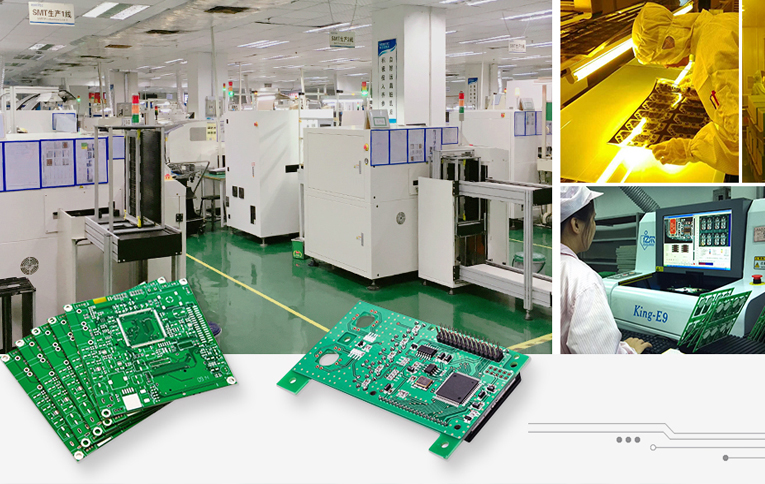
Solder paste jets printing is indeed the initial stage in the PCB assembly process. Solder paste is a mixture of tiny metal solder balls and a unique chemical that enables them to bond towards the printed circuit board's surfaces when warmed. The fluid is dispersed at quite a rate of 300 bits every second using only a solder paste jets printer. This technology provides for a better model and zero waste, as well as quick board changes and also no board transmission time.
Solder mask will only stay on the areas where parts would be mounted after administration. After that, a machine will check the PCB to confirm that solder paste has been put uniformly. A configured printed circuit board is just what's left after that.
The constructed PCB assembly process is subsequently delivered to pick and place machines with solder connected to predefined spots. Surface-mounted parts may be accurately moved onto a printed circuit board by a mechanical arm. Surface mount elements may be quickly attached to their exact places with this pick and place machine. The solder paste and elements are linked at this point, but they are not fused.
After the surface mount components have been installed upon that circuit board, the solder should be warmed to fuse these. A conveyor transports the printed circuit board to a "reflow oven," which warms the solder paste printing. Each side of this double Printed circuit board assembly will require independent solder stenciling and reflow soldering.
Just after the reflow procedure, the surface mount components are glued in line, but the PCB assembly process is not yet complete, and the finished board must be checked for operation. misplaced components during the reflow stage frequently lead to poor connectivity strength or even no connectivity at all. As displaced elements can occasionally join areas of the circuit that should not interconnect, flashes are a typical side consequence of this motion. surface mount technology may be used to look for these faults and malalignment.
The following are the most popular examination methods:
Manual inspections are still used in the PCB assembly process, regardless of the approaching emerging trends of automation and consistent supply. An in-person visual examination by a design is an efficient method of ensuring the integrity of a PCB following the reflow procedure for small volumes. However, even as the number of examined boards grows, this procedure gets increasingly more difficult and incorrect. For further than hours, looking at these simple sections might cause optical fatigue, leading to less precise examinations.
For bigger quantities of PCBAs, automated machine optical inspection seems to be one of the preferable inspection methods. An AOI machine, or automated optical examination machine a mechanical fixture, employs a variety of strong lenses to "view" PCBs. The AOI can detect a lesser solder joint because different types of solder joints reflect different light ways. The AOI does this at a rapid rate, allowing it to handle a large number of assembled PCB within a short period.
X-rays are still another form of examination. This is a less popular inspection procedure, and it's usually reserved for Boards that are more intricate or layered. The X-ray allows the observer to look through layers and perceive lower layers to spot any possible issues.
A defective board's destiny is determined by the Pcb assembly services requirements; it will either be sent again to be certified and rebuilt, or it will be discarded.
Through-hole components based on the kind of PCB assembly, the boards may have several components in addition to the standard SMDs. Plated tht components, or PTH elements, are an example. A plated through-hole in a PCB seems to be a hole inside the board that is plated well all way around. These holes are used by PCB component placement to transmit signals from one side of the board to the other. The soldering method will not work throughout this situation since it will run right through the hole without the need for an opportunity to attach.
PTH parts require a more specialized type of soldering procedure in the subsequent PCB fabrication process, rather than soldering paste
Manual through-hole implementation is a simple operation. One employee at a single station is typically entrusted with putting one component together into a specified PTH. The cycle repeats for every PTH that requires outfitting. Based on just how many PTH parts must be placed during one PCB assembly cycle, it can be a time-consuming operation. Most firms strive to avoid constructing with PTH components expressly for such a reason, yet PTH components are nevertheless ubiquitous in PCB assemblies.
Wave soldering is an automatic form of hand soldering, although the technique is significantly different. After the PTH element is installed, the board is placed on another conveyor line. Each time, the conveyor passes through a specialized oven, in which a wave of hot solder wipes over the board's base. This solders all the pins on the board's base at once.
For two-sided PCB assembly, this type of soldering is almost impracticable because soldering the whole PCB side will leave the electronic device worthless. After the soldering procedure is completed, the PCB can go to the final inspection, or it can repeat the functions and processes if the PCB requires extra components or the other side to be constructed.
After the soldering stage of the PCBA process is completed, the PCB would be tested for functioning. This is referred to as a "functional test." The testing puts the PCB throughout its length, imitating the regular operating conditions of the PCB. In this test, power plus simulated signals are sent across the PCB while testers examine its electronic engineering.
The prepared PCB fails the test if any of the properties, particularly voltage, power, or signal output, exhibit excessive fluctuation or reach peaks outside of a defined range. Based just on the firm's criteria, the faulty Printed circuit board assembly can either be recycled or trashed.
Technologies have become inextricably linked to our daily lives. In anything from cell devices to automobiles can be found in electronics components. The printed circuit board assembly, often known as a PCB, has been at the heart of such developments. With many moving elements, having printed circuit board assembly partners who not only know how your PCB assembly processes operate but also how to make it at the top class and lowest price is important. Imagineering Inc is a reputable PCB manufacturing in the United States.
Prev: PCB Design FAQ
Do you have any questions, or would you like to speak directly with a representative?