
Contact
Write to Us And We Would Be Happy to Advise You.
Do you have any questions, or would you like to speak directly with a representative?
By ren
Consider a world without the technologies we now take for granted, such as cell phones, computers, television, radio, automobiles, or airplanes. It would be impossible to attach electronic components to precise positions on devices or successfully connect the terminals of the elements in an ordered manner without the Printed circuit board layout. The truth is that most devices would not work without a decent PCB layout.
Creating a printed circuit board layout is analogous to finishing a work of art. Engineers may spend days, weeks, or even months developing these patterns to create something one-of-a-kind. However, it is not only engineers who can build a proper PCB layout; you can also go.
Routing can consume a substantial amount of computing resources. It is especially true for larger designs with three or four thousand components. When routing is challenging due to high component density, it can take a significant amount of time.
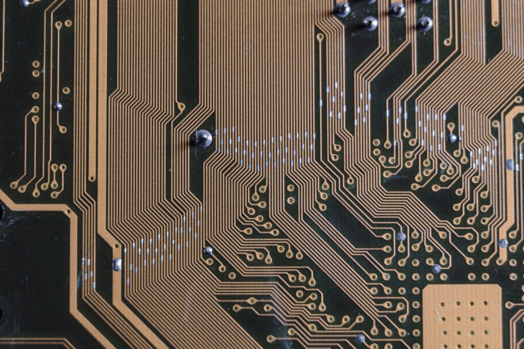
A layout, in general, refers to how the components of a particular item are set out or ordered. Similarly, a Printed circuit board layout is a broad phrase that refers to numerous stages involved in designing a PCB. It entails, among other things, producing traces, mounting hole cuttings, drill holes and surface mount components, labeling, and designating component placement.
Wire routing is one of the most fundamental ideas in PCB design. For example, the design software company claims that PCB design is 90.00% placement and 10.00% routing.
Routing is a phase that comes after placement. Determining the location of various components on the PCB is known as placement. Routing is connecting components by adding wires based on the design guidelines.
A PCB layout can be created in two ways: manually or automatically. The auto-router capability is available in almost every PCB design tool. Many designers utilize the auto-router device to save time and simplify the process.
Even though the auto-router function of PCB design is the most convenient, it is not always the best option. It is because it is not always as accurate and symmetrical as it should be. To ensure that automatic routing gives the best results, you must utilize the necessary parameters, which allow the automatic feature to compute the routes accurately.
Many computer-assisted design solutions are available because of the intricacy of commercial development programs.
Even for students and hobbyists, there are many excellent packages available for free or at a bit of cost.
The classic PCB design procedure of placing the tape on a master drawing sheet is gone, though it is likely still used in a few minimal circumstances.
The capability of PCB software varies greatly. The basic functionalities are provided by low-cost or even free software, while higher-end packages allow many additional features to be added to the design. Simulations, complicated routing, and a variety of other features are provided.
It would help if you first conferred with your producer before beginning to place components. It's critical to understand their requirements, such as the number of layers they can support. Other conditions could include minimum trace widths and trace spacing.
When electricity flows through the copper layers and copper traces, heat is produced. This heat must be controlled to not rise above a safe level. You may manage the heat by adjusting the width of the marks and ensuring that there is enough space between them; a procedure is known as PCB line spacing.
Line spacing might be challenging when dealing with a high-density interconnect PBC. Understanding several critical aspects of line spacing in these scenarios is vital.
The most crucial goal in PCB design is to include all of the necessary components in your PCB. To do so, you must first establish the spacing and angle of your lines.
Most designers employ either a 90-degree or a 45-degree angle; however, whether a 90-degree tip performs better than a 45-degree angle.
Schematic symbols and schematic diagram, a common ground terminal is always required. It is necessary for a Printed circuit board layout because it provides traces with a common reference point for monitoring voltages. Problems emerge when attempting to route to the ground using traces rather than ground planes.
Any provider of software, hardware, and intellectual property, recognizes three critical responsibilities played by the ground plane in PCB design:
The majority, if not all, of the components on the PCB are connected to a power net, and the ground net serves as a channel for the returning voltage.
Provides a path for signals to return so that they do not cause too much interference.
The large conducting area of a ground plane reduces disturbance since it has a lower impedance than traces used to route the ground net.
Overlapping planes are one of the issues in mixed-signal PCB layouts. A mixed-signal PCB layout combines digital and analog components on a single board. This overlapping could interfere with digital and analog signals if not appropriately controlled.
As a result, when it comes to Printed circuit board layout, you must prevent overlapping difficulties. According to us, you should always leave room between components.
Even though PCB layout is similar to art, it is critical to approach it systematically. The three phases listed below are essential for creating the most significant design:
Add and then rotate the components to lower the lengths and crossings of the air wires.
Electromagnetic interference is a common problem for PCB designers (EMI). EMI is "electromagnetic energy that affects signals in an electronic equipment by radiation or induction." "EMI is all around us," he continues, "from static on your radio to that buzz, you experience when you bring a cell phone near audio equipment."
Synchronous digital circuits are typically the most reliable signals on a PCB. As a result, radiated emissions can be seen in narrow bands. Furthermore, these peaks tend to occur at the harmonics of the clock's frequency.
Clocks are essential for distinguishing between pulses that define received or transmitted information. Many PCBs lack clock signals yet do include useful digital information.
Paying attention to the switching power circuit is critical in PCB design since a faulty power supply can result in a significant failure even if the course is constructed correctly.
By rapidly switching voltage levels in a transformer, switch-mode power supply and DC converters give several voltage levels. The switch circuit is programmed to use an ON/OFF feature based on a power range.
A functional layout is vital for the design and fabrication of almost anything. Similarly, having a good framework in place produces the desired results in PCB production. There are, however, a few flaws with the PCB design.
As would be expected in any case, using the incorrect instruments will yield the wrong outcomes. Some PCB designers utilize the wrong tools because they don't know any better. However, there are times when designers employ incorrect tools because they assume it will save them money.
If you choose the cheapest tools to save money, you may pay a lot more to fix the problem. You can avoid this problem by researching the best hardware and software for your PCB design project.
Making a PCB is not an easy task. The form and size of the PCB are two basic PCB design and layout factors. Complex PCB layout preparation issues involve designing the optimal layout between traces, trace lengths, and other elements that may affect board functionality.
The use of sophisticated software is typically used to solve layout preparation challenges. Using PCB designing services is another approach to benefit from the experience of organizations that have been in the area for a long time.
Read more: What is consigned PCB assembly?
Even though you can do your PCB designing, employing a PCB layout service has various advantages. These layout services can be beneficial, especially if you are new to this industry.
PCB layout services are offered for both existing and new PCBs. The following are some of the benefits of using PCB layout services:
When developing PCBs, having access to an expert is a significant advantage.
With PCB layout services, faults can be spotted and corrected early, allowing you to improve items before they are released to the public.
Layout services are of higher quality because every service strives to be better than the competitors.
With the help of an expert, PCBs can be designed on time based on meticulous planning.
Due to economies of scale, hiring PCB layout services may be less expensive than designing your PCBs.
PCB design is critical for board functionality. Assume you're having difficulty with your board arrangement. In that scenario, you may always seek help from a company that manufactures PCBs according to the best layout plans.
Ascertain that the organization appreciates the significance of a Printed circuit board layout for your boards to perform appropriately. We hope this article will help you know how to design a PCB; the printed circuit board layout, board outline, and integrated circuits layout.
Do you have any questions, or would you like to speak directly with a representative?