
Contact
Write to Us And We Would Be Happy to Advise You.
Do you have any questions, or would you like to speak directly with a representative?
By ren
When should you begin performing Design for manufacturing analysis on your design? Another critical question is: what is the best strategy to speed up the DFM analysis process? There is a lot to verify in each board, and thoroughly examining designs for manufacturability can take time, especially in complex layouts. Here's what to expect from DFM analysis and how to get your design through it as quickly as possible.
Design for manufacturing analysis, in general, applies to anything that must be mass-produced at a large scale. Manufactured products must be created to meet the high-volume production process; thus, a design must be examined to guarantee that nothing in the design will result in a low yield, faults, or lifetime.
DFM analysis for PCBs entails determining whether the design will comply with your manufacturing companies and assembly manufacturing processes. Any skilled designer should be aware that a lengthy list of alternative design decisions can jeopardize quality. We are aware that we haven't memorized every single manufacturability issue that could lurk in a design, so we frequently rely on my fabricator to review my boards when we are preparing to put in a fabrication run.
It raises an important question: when should you perform DFM tests on your design? If you're working on simple boards, it's usually fine to rely on your fabricator to run the last Design for manufacturing analysis before production; repeated DFM deep-dives waste time when your fabricator can do this quickly.
Numerous DFM analysis runs are required for more complex applications, such as high-layer count mixed-signal boards with tight clearances and multiple signaling standards, to detect potential quality concerns early.
A handful of these ideas are worth expanding on because they aren't commonly mentioned in other publications.

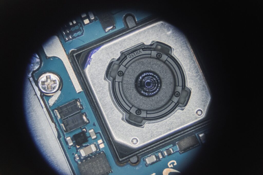
Some of the considerations that apply to connections also apply to other components, but there is a critical aspect about clearances worth noting. During assembly, check for expansion, especially on connectors with a plastic shroud or base. When two components are too close to each other and expand during soldering, they can lift off the board during the assembly process.
You should make an effort to ensure that your footprints are validated. It can be accomplished manually or by using only validated components directly from manufacturers when they are available. Once an impression is in the layout, you'll need to double-check solder mask holes, clearance to other members, and further details.
If you don't use software with proper rules-checking features, you might leave a thermal pad floating or place a drill hit too close to a solder fillet. You can examine the PCB layout directly, but it is entirely OK to generate preliminary Gerbers and compare your layers.
If you ask your fabricator for a stackup with your chosen layer count and layout, you'll pass this one with flying colors. They've already completed the Design for manufacturing analysis to verify that specified layer stacks pass through their product development process. They'll tell you what trace width, spacing (for differential pairs), and layer thickness you'll need to utilize with the laminate materials you've chosen. In some situations, you may be startled to learn that your preferred laminate material is unavailable and that you must substitute a close substitute.
For 4-layer stackups, you'll most likely get the conventional 8mil/40mil/8mil S/P/P/S stackup with a total thickness of 62 mil. More intricate stackups may necessitate the creation of a custom table, particularly if you have a board that requires impedance regulated routing.
If you acquire the stackup information early, you won't have to worry about using the improper trace and spacing for controlled impedance because everything has already been confirmed.
After completing your board and sending it for fabrication, your manufacturer should perform their Design for manufacturing analysis using your finalized Gerber files. Note that we say "should" since not all manufacturers will do this; for example, some manufacturers will accept your Gerbers and produce the board precisely as it appears in your fab files without question. Some manufacturers will require you to specifically request this level of service, as different service levels will only be available as an add-on.
When you receive your Design for manufacturing analysis from your manufacturer, you will see a lot of findings in two areas: clearance checks against process capabilities and clearance checks against specific industry criteria.
When you send your design files to your fabricator and perform their DFM analysis, you'll most likely get a lot of findings centered on clearance checks. The fabricator should already examine the locations mentioned above, but they should also compare your feature sizes and clearances to their process capabilities. Even though you went through this process with early Gerbers as part of the pricing process, it's essential to rerun it because you may have missed something.
We can see the spacing, annular ring diameters, and clearances between the plated through-holes and the copper. The trace-to-copper clearance setting is too low, as evidenced by the bottom row, and the pads on some footprints have small annular ring diameters.
How does your fabricator check every potential aspect of your PCB layout for a vast, complex design with thousands of nets? Some tools can help automate this procedure and generate a report detailing any process violations. Some manufacturers have programs that they will utilize internally. Still, others will provide you with access to a downloaded tool that you may use to test your design before additive manufacturing.
A review of conformity with IPC Classes is another area of design criteria that may necessitate more skill. One critical element to specify during the quoting process is the level of IPC qualification you require if any.
You are checking for teardrops, annular ring widths, drill and pad diameters vs. copper weight, ability to plate vias and holes, and dielectric thickness requirements, to name a few of the most crucial dependability requirements.
The physical layout will be compared to fabricator capabilities to ensure that the finished design meets the certification and performance requirements established in IPC standards, and revisions will be required before fabrication.
What is the quickest way to send files to your manufacturer, and how can you assure they completely grasp your design intent? You'll need the best cloud collaboration tools available.
With everything being done these days digitally, PCB designers want tools to assist them in collaborating on complicated projects and sharing them with their manufacturing partners. Everything from whole project releases to individual design files may be shared swiftly with your manufacturer, other team members, and customers.
Once your design is with your fabricator, they can comment on specific design aspects, reducing confusion when reading a DFM analysis report.
When the designer has access to Design for manufacturing analysis, it can be done at strategic points in the design flow. Because of the direct interaction between the engineer and the analysis, the organization executing the design determines when it is ideal for conducting the DFM tests.
There is no need to interact with outside providers who may make such decisions based on competing priorities. This method also permits the analysis to be performed early in the design phase rather than a nearly completed design.
However, one more change can be made to allow the designer to apply a correct-by-construction methodology while actively developing the PCB utilizing DFM rules.
A correct by construction technique replaces the usual and iterative design-then-check-then-design procedure for DFM with dynamically applied production rules during layout. Design for manufacturing analysis can be performed at strategic points in the design flow when the designer has access to it.
Because of the direct contact between the engineer and the analysis, the organization implementing the design selects when the DFM tests should be performed.
There is no need to engage with third-party suppliers who may make such decisions based on competing priorities. This method allows the analysis to be completed early in the design process rather than a nearly finished design.
The ultimate purpose of a left-shift program is to enable the design system to support a correct-by-construction methodology based on DFM rules, hence it is to reduce manufacturing costs post-design iterations. The ultimate accomplishment of this method is the creation of a PCB design flow with a fully integrated manufacturing analysis that aids the designer in completing the assignment while being transparent to the overall layout process.
Europepcb is a front-runner marketplace in DFM analysis. Our engineering and industrialized knowledge empowers us to predict the processes needed to generate a practical design precisely. We employ people from manufacturing operations, the right manufacturing process tooling, and processing disciplines for a higher approach to align our skills with your aims.
The significance of Design for manufacturing analysis is consequent from the prominence placed on classifying practical explanations to plan barriers that could threaten successful consequences. DFM analysis recognizes forecasts for manufacturing cost-saving and raw material cost-saving, enhanced manufacturability, and earlier time to marketplace.
We hope this article will help you engross the side-to-side knowledge for design for manufacturing analysis; know the factors to; reduce cost (part cost, overhead cost), and have significant savings, design stage, injection molding.
Do you have any questions, or would you like to speak directly with a representative?