
Contact
Write to Us And We Would Be Happy to Advise You.
Do you have any questions, or would you like to speak directly with a representative?
By ren
.
Double layer PCB manufacturing is quite simple and involves several stages. The first and most important is design and stacking. It is not a difficult task to stack up a double-layer PCB. In simple words, you must stack single-layered PCBs with each other.
It consists of two layers. The upper and lower layer is made of Cu and is electrically connected to each other. We can also use silver- or gold-plated layers to enhance the properties.
After the top layer comes an insulating material or dielectric. This is considered a base where both layers are connected. This can be of any type of material either polymeric or metals. These include polyamide, polyimide, PTFE, or metals like Cu, Al, Fe, Ag, etc.
If the base is conducting in nature i.e., metal then insulation is created among layers by using a dielectric medium. While non-conductive base material, it acts as an insulating medium between the top and bottom layers.
There are other layers other than these conductive and base layers. They are present in all types of PCBs and give them extra advantages. These are silkscreen, solder mask, and surface finish. Their function is to label components, avoid the creation of solder bridges and produce a copper layer and protect it from corrosion respectively.
Double layer PCB is divided into several types depending on their functioning, properties, and applications. These are:
The designing process of a 2-layered PCB is quite simple and doesn't require any effort. The designer will select software like EDA, CAD, or MAT- a lab of his own choice depending on the requirement. We must follow some steps for this purpose. They are as follows:
Then, your required design of Double-sided boards is ready.
The material used in the production of 2- sided PCB is prepared by the manufacturer. Copper-clad-epoxy glasses are used as raw material for PCBs. Materials like FR-4, iron and ceramic substrates, and polymeric materials.
After selecting the raw material, cut the board according to the required size. It is cut according to the machinery in which it is used. It should be cut larger than the size of the circuit. The size of the PCB should be small to make it cost-effective and fit multiple circuits on both sides of the board.
This board after cutting undergoes a drilling machine to create small holes on it.
Manufacturers process drill panels with the help of a deburring machine. They are then passed through abrasive materials or brushes causing the removal of copper plating and fingerprints from the surface. Deburring also causes the removal of oxides from the surface creating a shiny and smooth surface.
Initially, holes in electroless copper deposition are composed of epoxies. To prevent oxidation and protect the surface from corrosion board is dipped in acid solutions.
This consists of two types i.e., Vertical & Horizontal. Horizontal plating through holes is done for the deposition of Carbon while vertical plating is for copper on both sides of the board.
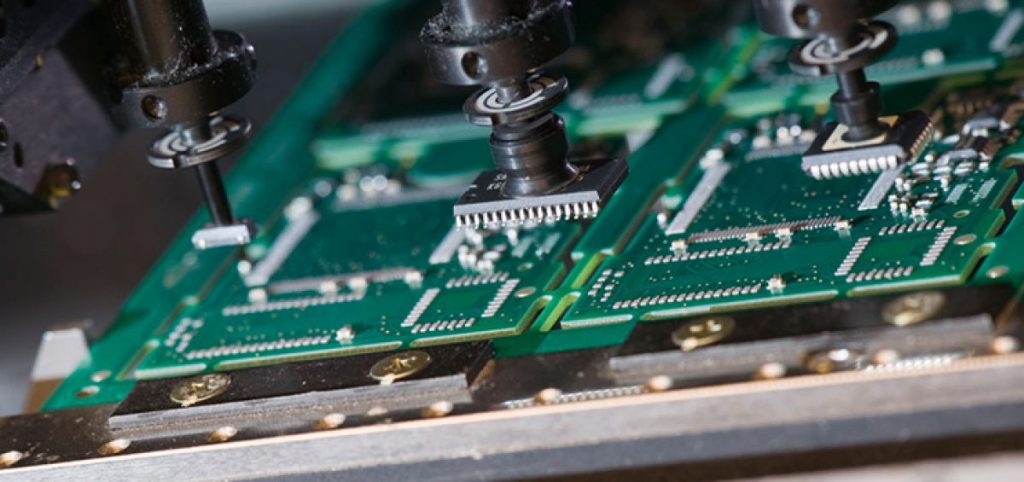
The negative image of a pattern on the circuit board is transported to the panel.
Panels are dipped into etchant which removes exposed Cu but doesn't react with Pb which is protecting the Cu surface after this layer.
It is present on the whole circuit thus protecting it and avoiding the short circuit formation.
Different surface finishing techniques are used to create a smooth and shiny surface like HASL, ENEG, ENIG, etc.
Nickel- and gold-plated surface provides protection against the external environment and provides good heat and corrosion resistance.
The application of components on the surface of a circuit board is named as silk screen. It is also used to insert a logo as well.
Boards are separated into pieces by cutting them.
A flying probe test is performed to check the working of a printed circuit board.
The board should be cut larger than the size of the circuit. The size of the PCB should be small to make it cost-effective and fit multiple circuits on board.
It is one of the most common and widely used types of PCB because it can be used in complex designs and have good flexibility. Some advantages of 2-layered PCB are given below:
Double-layered PCBs have a high compact density, and hence more components can be compacted easily in a small space. Since both PCBs are used so we can place the components on both upper and lower sides.
We utilize both sides of the board to make it more compact and include many components to enhance its working. While in the case of a single-sided board, one side is not occupied and hence not used for complex applications.
Although it consists of two layers but occupies less space compared to single-layered PCB. Due to its compactness and high density, each part of it is consumed properly.
If you are looking for more advantages on less budget, then double-sided PCBs are the best option. There is no need of wasting a handful amount of money on single and multi-layer PCBs. It offers circuit implementation on both sides using little space and money.
Single-sided PCBs and multi-layer PCBs are not designed in such a way that a complex design can be implemented. Moreover, they offer several good properties and functions at a very low cost. That’s why they have widespread uses in electronic components and appliances.
The circuit board of a double-layer PCB has metal on its sides, a high transition temperature Cu board, flexibility, and high frequency that makes it suitable for complex design applications of double-sided PCB.
Several surface treatments are performed for manufacturing double-layer PCB board models. These techniques include immersion gold, Pb-free Sn spraying, etc.
Double-layer PCBs are used in all types of our daily use devices like electronics, juicers, and LED lights because of their low cost and ability to fit in complex designs. Also, for heavy appliances like converters, UPS, inverters, HVLS fans, coolers, instrumentation, etc. Their demand has increased due to the increased requirement for renewable energy.
If you want your products to be of high quality, make sure you connect to a good service provider. All the design and manufacturing process is although bit easy, but it requires experts and professionals to make sure that the final product is capable enough to be launched in the market.
Does it meet all the standards? If you want professional behaviour and good service, then here is good news for you because Europe PCB is known to provide the best services and they are known as one of the great service providers of PCB assembly manufacturers all around Europe and provide their services in SMT & DIP and much more.
So, what are you waiting for? Get your orders placed now and enjoy the best services.
Do you have any questions, or would you like to speak directly with a representative?