
Contact
Write to Us And We Would Be Happy to Advise You.
Do you have any questions, or would you like to speak directly with a representative?
By hqt
The base is made of insulating material made of dielectric having good strength.
This layer is usually made of metals and serves as a base for other layers like solder masks and silk screens.
Only one layer of conductive material, made of copper is present. A layer of solder mask is present on top of the copper layer. This copper foil provides protection against the external environment.
Any type of material like polymers, metals, and composites can be used depending on the properties required. The most widely used materials for single-sided PCB are as follows
Now we will discuss the types of one-sided or single-layer PCB layers depending on their rigidity, flexibility, frequency, etc.
As the name suggests that this single-layer PCB is made of rigid material. Fibreglass is usually the preferred material in this case. This rigidity and inflexibility provide the circuit with adequate strength and prevent it from bending. It is used in power supplies, calculators, and other electronic equipment.
This type of single-sided PCB uses flexible and elastic materials such as plastics. Due to its elastic nature, it is preferred over rigid single-layer PCB. But it is expensive because of the fabrication process.
It is the type of single-layer PCB having high frequencies and usually in terms of Gigahertz (GHz). Polymer materials like Teflon and polyphenylene are used. Other factors like the coefficient of thermal expansion, and water absorption can affect the frequency of single-sided PCB. So, they should be kept in mind accordingly.
This type of single-layer PCB is a combination of both rigid and flexible materials like fibreglass epoxy resins and plastics. Since this sandwich of hard and flexible materials provides good properties as compared to other types of single-layer PCBs. It can also be used to reduce the mass-to-weight ratio.
This layer consists of Aluminum as a base material. Its design is similar to that of Cu-supported PCB, but the only difference is that the material used is aluminium. Moreover, Al is a cheap material with good heat-resistant properties.
For designing a material, its thickness, width, diameter, etc. plays an important role in its applications. For this purpose, it is likely to know the thickness of single-sided PCB for its better functioning. There are international standards like ASMI, ISO, etc. that guide us on how much thickness is required for certain applications.
For example, a rigid single-sided printed circuit board has a large thickness as compared to the flexible one. This shows that some devices require a small thickness while others require a small thickness up to a few mm.
Industries usually use a thickness of about
The standard thickness used in single-sided PCBs used in industries is about 1.57 mm (0.063 inches).
Nowadays, less thickness and more flexibility are preferred. Also, people demand small and light electronic equipment that can be easily installed in devices. So, thickness range from 0.2031 mm to 6.097 mm.
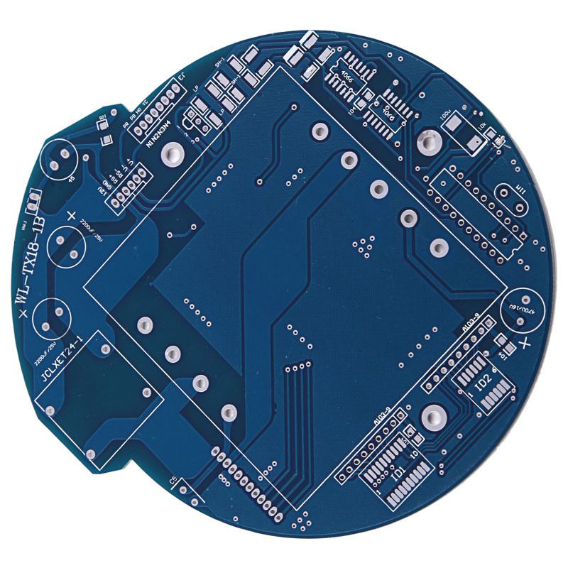
Manufacturing of single-layer PCBs is a long process because it requires processing and preparing material from scratch.
The processes involved in manufacturing are:
Material is cut with the help of machinery according to the design.
The PCB board is properly cleaned to avoid contamination and to ensure the quality of the product)
Holes are drilled to add components to the board.
It is done to make it conducive for certain materials and avoid contact with unwanted substances
After electroplating, the material is checked properly by using highly precise inspection methods
If you want to create a circuit pattern on a PCB board, apply a light resistive film to the surface. This occurs when no light can be entered. It is then passed through UV light and the resistive film gets hardened and produces the required design.
Removal of unwanted copper by using the highly alkaline solution and the circuit is hardened using UV rays
It is an excellent way to determine errors by using optical devices and X-rays
It is a thin polymer layer available in different colours. Customers can choose the colour according to their own choice. It makes the surface attractive and appealing and protects it from the formation of solder bridges on the board.
It is used to print labels on the board and also proves to help determine the wrong displacement.
The surface finish can be according to your choice. You can use HSLA, LF HSLA,ENEPIG etc.
It is done to make sure the working of product.
Single layer PCB has a wide range of applications. Most of the devices that we use in our daily life use single-layer PCB. Some of them are :
Advantages and disadvantages:
Advantages:
Single-layer PCB design is very simple and consists of only a single conductor. It is easy for the designer to design reducing the risk of errors. So, we get quick results in a single attempt.
Due to its simple design and fast manufacturing process, most manufacturers provide this service. It is almost available in every city or country.
Single layer PCB is the best choice if you want more on a less budget. Because of its low manufacturing cost and cheap material, it is also not expensive. Moreover, if you order in bulk you can also get your cost reduced further.
Long lasting nature of materials makes them more attractive. It provides excellent reliability because during production and design it can be easily prepared with little chance of error. The board and components' long-lastingness is guaranteed.
Processes like drilling, cutting, and soldering can be easily performed.
Inspection of single-layer PCB is easy as compared to multi-layer. They can be easily tested by using the optical inspection method or X-ray. Less effort is required in repairing because of the simple design.
Disadvantages:
It is a single layer and is extended in several dimensions. So, it requires a large space on the board.
Everything has certain limitations and not everything we require can be achieved easily. We cannot use single-layer PCBs in the case of circuits that have a complex design.
It has a very slow speed of transmission of electrons and signals. If you want high speed, then a multi-layer would be more suitable for you.
Why you need a good single-layer PCB service provider:
If you want your products to be of high quality make sure you connect to a good service provider. This process is although bit easy, but it requires experts and professionals to make sure that the final product is either capable enough to be launched in the market.
Does it meet all the standards? If you want professional behaviour and good service then here is good news for you because Europe PCB is known to provide the best services and they are known as one of the great service providers of PCB assembly manufacturers all around Europe.
Europe PCB will provide you with highly satisfying products with good customer service as well.
So, what are you waiting for? Get your orders placed now and enjoy the best services.
Do you have any questions, or would you like to speak directly with a representative?