
Contact
Write to Us And We Would Be Happy to Advise You.
Do you have any questions, or would you like to speak directly with a representative?
By hqt
There is an opinion among my friends that it is useless to make printed circuit boards (PCB) on your own. Considering that modern components have gone far from DIP cases, it is not even worth trying to use artisanal etching boards for them. Nevertheless, there is always a need for a quick assessment of a particular component, and there is no time to wait for the ordered payment for several days. And this is taking into account that the order for "several days" is expensive, for a one-time task.
In this article, I want to outline the procedure that will allow you to quickly manufacture PCBs for components in packages similar to the TQFP-100, that is, with 0.2mm legs and the same clearance, and at the same time minimize rejects.
Of course, this is a method of making boards only for prototypes, but it reduces the risk of mistakes when creating the final device.
There are many articles and videos with similar advice on the network, but as a rule, all the nuances of certain actions are not covered there. Here I want to show the whole process, which at home will make it possible to make an acceptable copy of the PP in an hour and a half.
Details and traffic under the cut.
Minimum set of materials:
And, of course, a laser printer and an iron.
I will show the whole process on the manufacture of the PCB for the evaluation board of the ATxmega128A1U-AU microcircuit (evaluation of the declared hardware crypto module, EBI and in general), and the board for connecting a 7-inch display to the STM32F407VE
For evaluation boards I try to make the wiring only on one side, where intersections cannot be avoided , put a resistor with resistance = 0 and case 0805, passing the road under it. If there are a lot of intersections and you definitely need two layers, then I etch each layer on a separate PCB (I then connect using VIA).
PCB preparation.
One-sided textolite with a copper thickness of 17-35 microns is washed from dirt with dish soap under warm water, then a drop of detergent is applied to a sandpaper with a grain of P800 or less, and the future board is sanded until roughness is formed over the entire area. The moment with the skin is a must! In this way, the copper will not rub up to the holes, but we will ensure good adhesion of the toner. After sanding, the surface is washed with clean water, wiped dry and set aside to dry.
By the time the layout is transferred, the textolite must be dry, free of oxides, greasy stains and noticeable roughness.
In one of the articles I saw a recommendation that the copper layer should be kept in the sun until a gray oxide film appears, in our case this is not necessary.
Preparation of the layout.
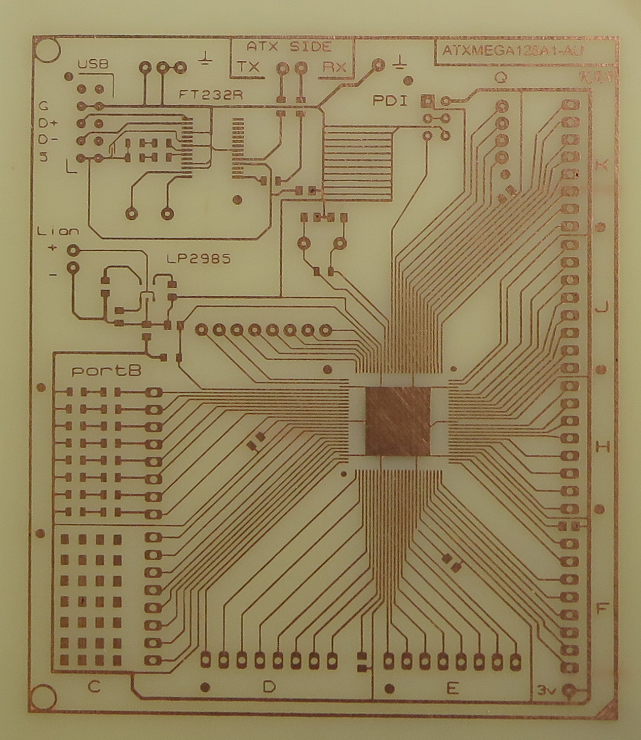
For ATxmega128 I made the following layout:
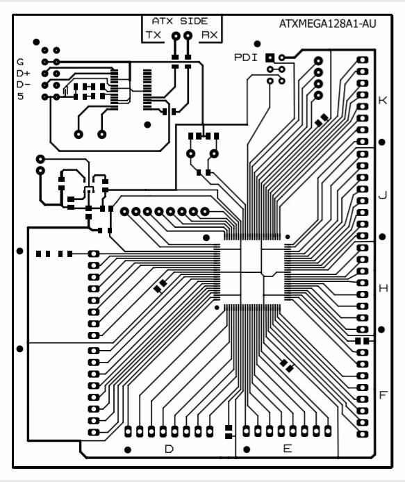
On the board is the xmega itself, the ft232 interface converter and the lp2985 stabilizer, as well as small things - the PDI connector, USB, LEDs for the entire "B" port. The board drawing is somewhat different from what I will etch. Before printing, I added inscriptions and little things for complication.
All roads are on the top layer (TOP), so we print the layout in a mirrored form.
The printer does not need to have a "waste" mode for bold printing. I printed on different printers with printing "by default" and there were no problems, except for one point: Brother printers (specifically HL-l2340 and HL-l2250) are very disrespectful to DPI conversion to real size, so the picture can float in size , and this is critical when two roads must fit 1mm.
Now the paper.
No glossy magazines or self-adhesive backing!
And I also refused even from Chinese paper for LUT (it is too thin and wrinkles when printing) The
paper should be dense - at least 150 grams per square centimeter, should quickly stick when heated and not fidget under the iron, swell well in water.
The best option is glossy photo paper, not very good quality. Not "too good quality" means not premium and not LOMOND. That is, cheap glossy photo paper. In the photo above, one of these is shown, there is also “Glossy Photo Paper” produced under the brand of a large computer equipment store, this is a clone of the one in the photo (it seems that they are from the same plant, but in different packages).
This paper immediately adheres to copper under the iron and does not move when ironing (matte paper does not contain a glossy layer and therefore does not stick, and hot toner is easy to smear), it easily comes off in warm water (unlike LOMOND and paper with the prefix "premium" ).
So it's time to print. We print the layout, then, without touching the front side with our fingers, we cut off the edges. and prepare the iron.
Translation of the layout.
You must first prepare a container with water in which the board will be soaked. For me, the role of this container is performed by an ordinary basin. Hot water is poured (50 degrees, that is, so that the hand can no longer tolerate), five liters, and a little detergent dissolves in it (a little, it's a tablespoon).
And we go to the iron.
We put the prepared textolite on a flat surface and cover it with a printed layout, iron heated to the maximum temperature along the center line, and then from the center to the sides. When ironing for the first time, it is better to hold the printout so that it does not move. After the first ironing, a sheet of photographic paper sticks to the copper and you can no longer be afraid to move it with an iron. Now you can use the tip of the iron to walk along all the edges and places where the paper looks like it is coming off. Then we just warm up for about thirty seconds throughout the entire volume.
I could not resist not to show the main character in the article about LUT:
After ironing, without cooling, we throw the board with water. That is, without removing the paper, we pick up the hot one with tweezers and put it in a prepared container with water. 10 minutes soak break.
Cleaning from paper.
After 10 minutes, we take the board out of the water and remove the paper. No matter how long the board is in the water, all the paper will not fall behind. More precisely, the paper itself is without problems, but the glossy layer, which provided us with good adhesion, will remain in narrow places.
Something like this:
In general, the toner holds very reliably, you can rub it with your fingers, an eraser or a dishwashing sponge, but it is difficult to pull out the gloss between the tracks, it is enough to let the board dry, as such places will be visible.
There are three ways.
To do this, you need to wet the board back and remove the excess with a sharp object. It is best to use a sharp toothpick. Wet gloss can be removed without problems, and the wood of the toothpick does not wear off the toner. Note that you cannot use needles! Not because the toner can be removed (it stuck well), but because the iron leaves traces on the copper. Yes! I myself am in shock, I know that copper is softer than iron, especially stainless steel. But the fact takes place. Where the needle drove, copper is etched very slowly.
Practical example:

After removing the remains of the glossy layer, rinse the board with detergent, removing the "fingers". Leave to dry.

Almost deliberately left a few places where the gloss was not removed (later we will see that everything is not so scary).
Etching.
I poison with ammonium persulfate, I won't say that it is better than ferric chloride, just more dirt from iron (well, yes, ammonium persulfate is a bleach, what kind of dirt is there) and ferric chloride is more difficult to store - it is hygroscopic and, as a result, fuses into large pieces that need to be crushed ...
I bait at a temperature of 40 degrees. On a board with copper 35 microns - 15 minutes, with copper 17 microns - 5 dashes 7 minutes. It is possible and at room temperature 17 microns is etched for about 20 minutes, 35 microns in theory 40 minutes, but I don't remember that anymore.
At home, you can pickle in any container, for this article, I specially pickled it in an ordinary plastic container, which imposes certain additional actions from the performer. But if PPs are made often, then you can close up an etching bath for yourself:
the main addition of which is a pump for mixing the solution, it frees from "certain additional actions". You need a diaphragm pump with a plastic diaphragm.
The one in the picture was bought in an online store for robocrafters.
There is a partition inside the container for placing several PCBs.
In the photo, two sides of the board are etched under the STM32F407VE connected to a seven-inch display.
Under the xmega I will etch in an open plastic.
We make a solution - half a liter of water plus 100-150 g of ammonium persulfate. In general, 250 grams per half liter is recommended, but in artisanal conditions, when the solution cools and the water evaporates, crystals fall out and stick tightly to the copper, as a result, non-etched points.
As I wrote above, the temperature is 40 degrees.
We throw a board into the solution and begin to mix the solution with a brush so that the etching goes evenly. You can also use a brush to remove flakes of a glossy coating from the board, if not all of them were removed during preparation.
I have a board with copper 35 microns, after 10 minutes the textolite is already visible:
I wait another 5 minutes and everything is ready.
I must say that during the etching process, it is better to overexpose the board than underexpose. And the extra time can be quite large. Once I saw the non-etched landfill and threw the handkerchief back and forgot about it for about three hours, when I remembered that it had been eaten through and through. However, I did not notice a single poisoning:
this overexposed one (already tinned):
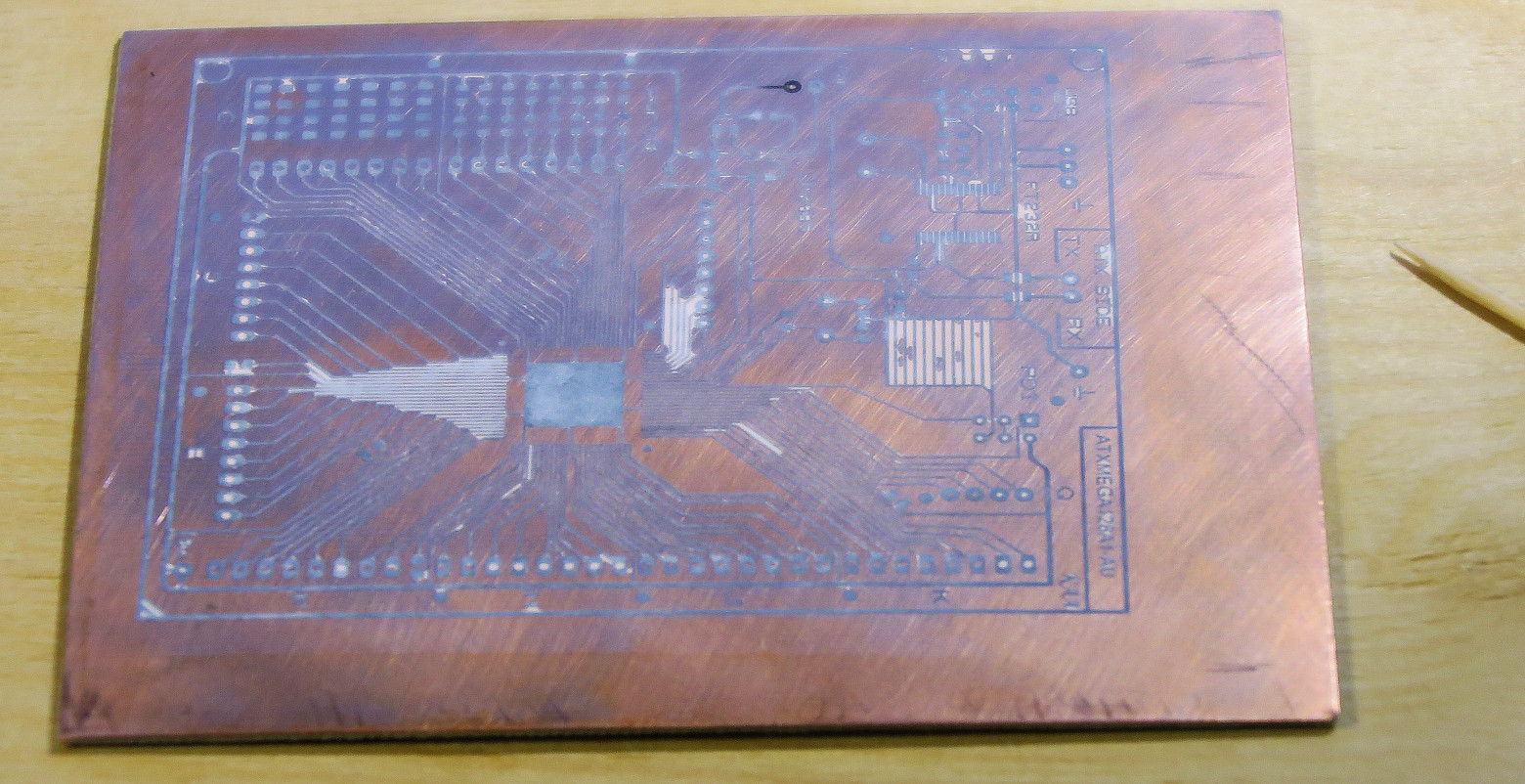
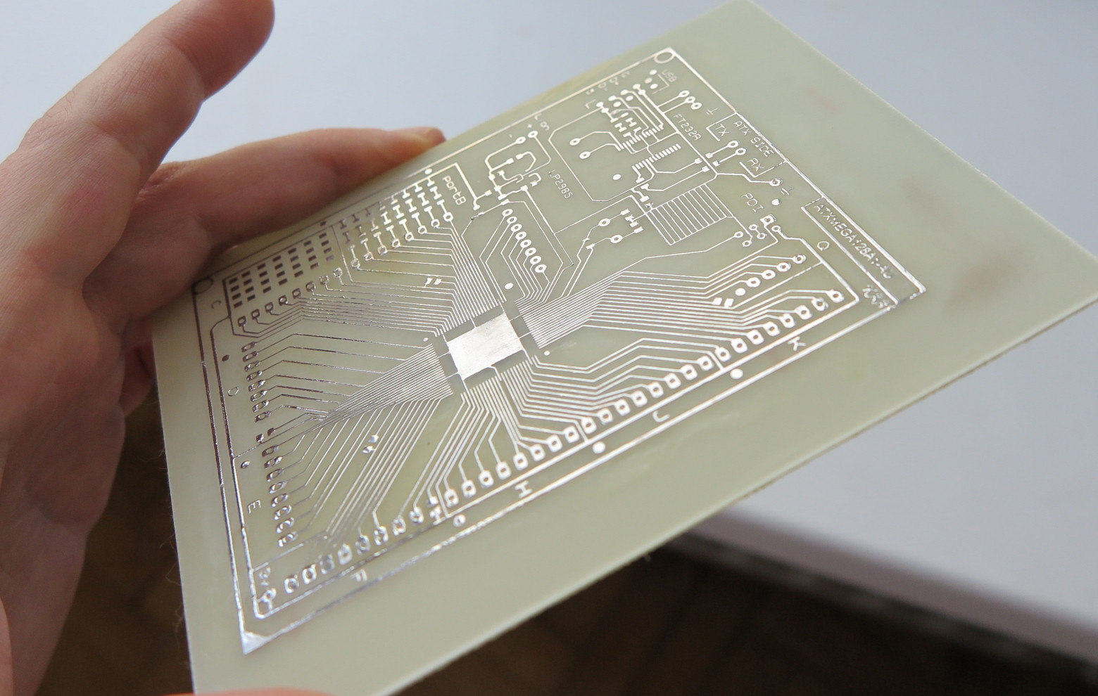
So, they took out our board, washed it and looked at the light:

If you found excess copper, you can throw it back into the solution.
If all is well, then the LUT is over!
We wash off the toner with acetone and service it, if maintenance is not provided in the near future, then you can store the board without washing off the toner, it will be a protective shell.
Bottom line:
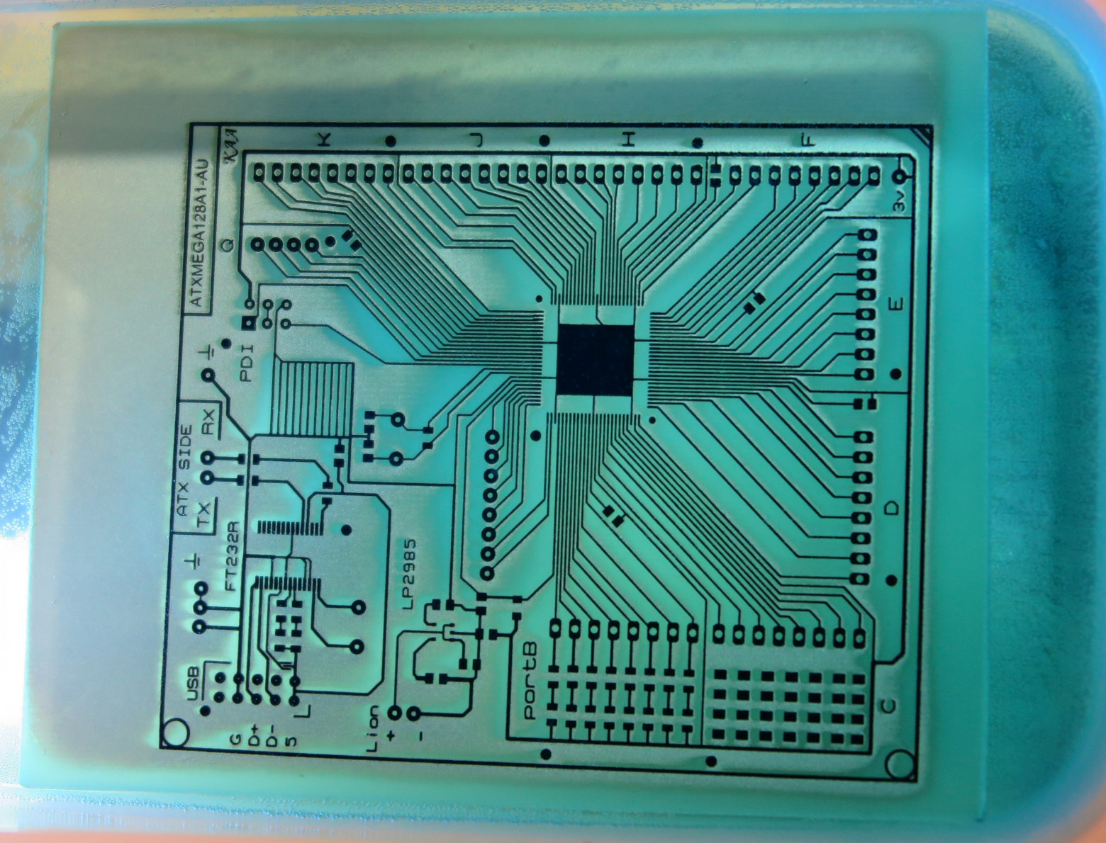
Above, I marked the places on the board where the glossy coating remained. The places that the gloss covered hermetically (the corner on the board) did not etch there, where there are small overlaps between the tracks - everything is fine, the solution made its way there. If you use a container with a pump, then the glossy coating can not be completely wiped off at all, just the etching time is doubled.
A couple of phrases about tinning. Since LUT makes boards that are temporary or for yourself, it is not worth bothering with maintenance (IMHO), you can just walk with a soldering iron through those places where there will be soldering, and then varnish everything.
But if the components on the board will be re-soldered or the board will be in use for a long time, then it is better to tin it. Either go through the entire copper with a soldering iron, or if there is a hair dryer, then with solder paste.
I mix the paste with the flux with about 1 part of the paste and 5 parts of the flux, cover the entire board and heat it up with a hairdryer:
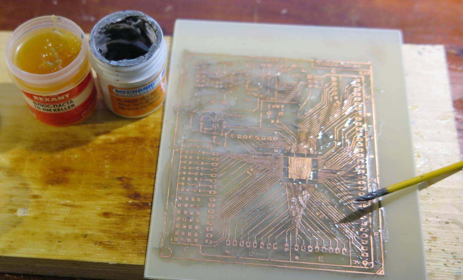
during heating, I use a textolite brush (known as an "eternal brush") to drive the solder to the edges of the board. There is no excess solder on the tracks with this method , and where it is not enough, you can drive from the edges. Not an air knife, of course, but also pretty neat.
The main problem when using solder paste is the extra balls that are stuck to the board. You can clearly see them in the photo:

Therefore, after tinning, the board must be thoroughly rinsed and wiped off with a cloth dipped in acetone.
The board was irradiated, now everything is for sure. Mounting. Check:
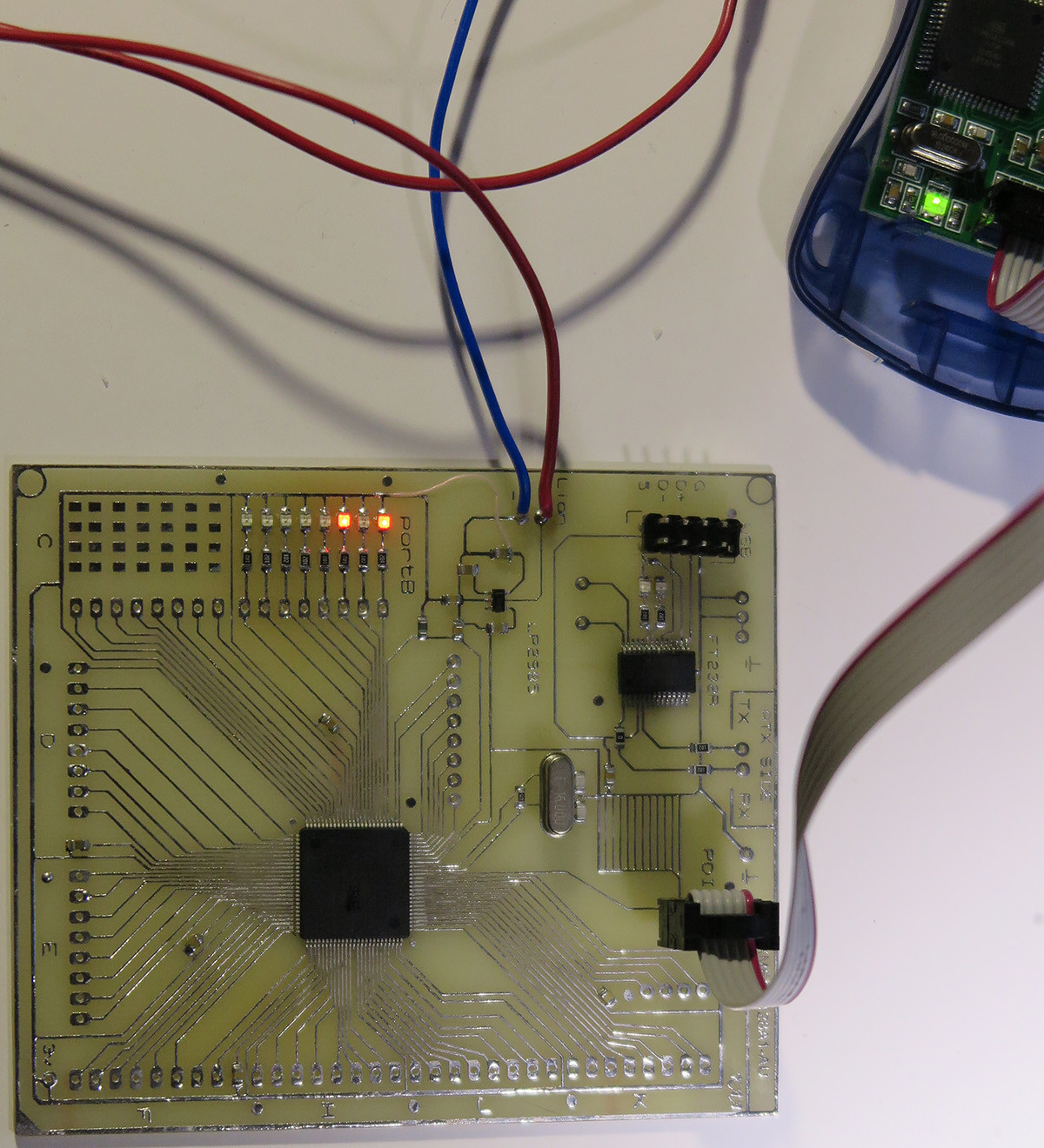
Task completed. This board took no more than an hour (taking into account photographing the stages).
At the same time, a second board was etched, or rather two sides of one board. And if the first scarf was more likely for a demonstration (it was possible to do it on a DIP adapter, and not to do something like an arduina), then the second one was needed for a specific purpose and weaving braids of wires on the adapter is not an option (and it’s not a fact that there is no interference with connection via fsmc)
Two sides:
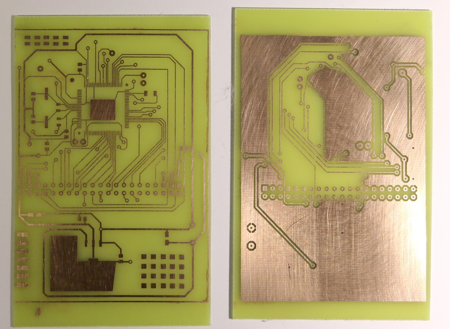
As you can see, I did not etch double-sided textolite, going through the deadly procedure of combining two templates at the stage of working with an iron. Better to do it now.
We drill holes on the VIA for all the boards, take the legs from the resistors and solder 5 pieces to one side, then string the other side on them, solder them on both sides. All boards are combined! All holes can now be soldered.
Something like this:

Everything is ready!
You must have noticed a strong defect on one of the sides: The

paper after the printer is electrolyzed and collects everything. Especially hair, especially cat hair! So I didn’t finish watching.
And here is the culprit:

Controls all running processes.
After the restoration of the track, the PC is ready and the device is assembled:
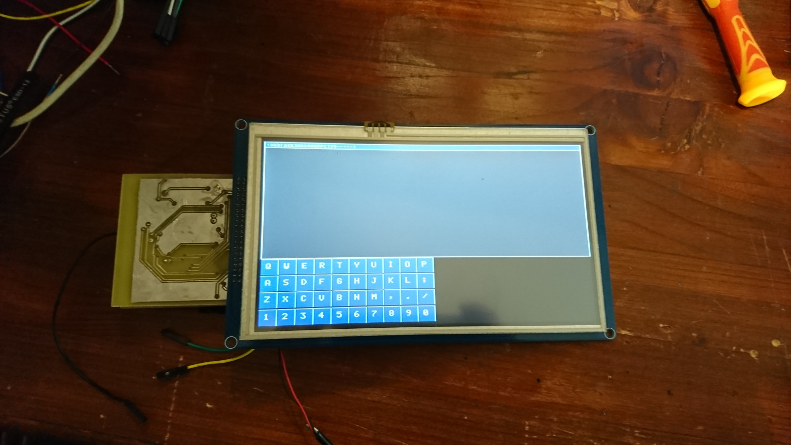
True, it was just a temporary board - to check the correctness of the connections, so that later it could be bred humanly and ordered.
Prev: Zenit PCB
Next: LED PCB MEASUREMENT
Do you have any questions, or would you like to speak directly with a representative?